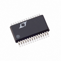
LTC3728EG Linear Technology, LTC3728EG Datasheet - Page 9

LTC3728EG
Manufacturer Part Number
LTC3728EG
Description
IC SW REG SYNC STP-DN DUAL28SSOP
Manufacturer
Linear Technology
Series
PolyPhase®r
Type
Step-Down (Buck)r
Datasheet
1.LTC3728EGPBF.pdf
(36 pages)
Specifications of LTC3728EG
Internal Switch(s)
No
Synchronous Rectifier
Yes
Number Of Outputs
2
Voltage - Output
0.8 ~ 5.5 V
Current - Output
3A
Frequency - Switching
250kHz ~ 550kHz
Voltage - Input
3.5 ~ 36 V
Operating Temperature
-40°C ~ 85°C
Mounting Type
Surface Mount
Package / Case
28-SSOP
Lead Free Status / RoHS Status
Contains lead / RoHS non-compliant
Power - Output
-
Available stocks
Company
Part Number
Manufacturer
Quantity
Price
Company:
Part Number:
LTC3728EG
Manufacturer:
MAXIM
Quantity:
158 341
Part Number:
LTC3728EG
Manufacturer:
LT/凌特
Quantity:
20 000
Part Number:
LTC3728EG#PBF
Manufacturer:
LINEAR/凌特
Quantity:
20 000
Company:
Part Number:
LTC3728EG#TRPBF
Manufacturer:
LINEAR
Quantity:
63
Part Number:
LTC3728EG#TRPBF
Manufacturer:
LINEART
Quantity:
20 000
Part Number:
LTC3728EG-1
Manufacturer:
LINEAR/凌特
Quantity:
20 000
Company:
Part Number:
LTC3728EGTRPBF
Manufacturer:
LINEAR
Quantity:
1 350
PIN FUNCTIONS
INTV
Low Dropout Regulator and the EXTV
and control circuits are powered from this voltage source.
Must be decoupled to power ground with a minimum of
4.7μF tantalum or other low ESR capacitor.
EXTV
Internal Switch Connected to INTV
and supplies V
out regulator, whenever EXTV
EXTV
7V on this pin.
BG1, BG2 (Pins 23, 19/Pins 22, 18): High Current Gate
Drives for Bottom (Synchronous) N-Channel MOSFETs.
Voltage swing at these pins is from ground to INTV
V
tor should be tied between this pin and the signal ground
pin.
BOOST1, BOOST2 (Pins 25, 18/Pins 24, 17): Bootstrapped
Supplies to the Topside Floating Drivers. Capacitors
IN
(Pin 24/Pin 23): Main Supply Pin. A bypass capaci-
CC
CC
CC
(Pin 21/Pin 20): Output of the Internal 5V Linear
connection in Applications section. Do not exceed
(Pin 22/Pin 21): External Power Input to an
CC
power, bypassing the internal low drop-
CC
is higher than 4.7V. See
CC
CC
. This switch closes
Switch. The driver
CC
.
are connected between the boost and switch pins and
Schottky diodes are tied between the boost and INTV
pins. Voltage swing at the boost pins is from INTV
(V
SW1, SW2 (Pins 26, 17/Pins 25, 15): Switch Node
Connections to Inductors. Voltage swing at these pins
is from a Schottky diode (external) voltage drop below
ground to V
TG1, TG2 (Pins 27, 16/Pins 26, 14): High Current Gate
Drives for Top N-Channel MOSFETs. These are the out-
puts of fl oating drivers with a voltage swing equal to
INTV
SW.
PGOOD (Pin 28/Pin 27): Open-Drain Logic Output. PGOOD
is pulled to ground when the voltage on either V
pin is not within ±7.5% of its set point.
Exposed Pad (Pin 33) SGND: The Exposed Pad must be
soldered to PCB ground for electrical contact and rated
thermal performance.
IN
+ INTV
CC
– 0.5V superimposed on the switch node voltage
CC
IN
).
.
LTC3728
OSENSE
CC
3728fg
9
CC
to


