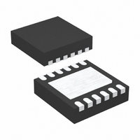
LT3500HDD#TRPBF Linear Technology, LT3500HDD#TRPBF Datasheet - Page 8

LT3500HDD#TRPBF
Manufacturer Part Number
LT3500HDD#TRPBF
Description
IC REG STP-DWN 2A 12-DFN
Manufacturer
Linear Technology
Type
Step-Down (Buck)r
Datasheet
1.LT3500EDDPBF.pdf
(28 pages)
Specifications of LT3500HDD#TRPBF
Topology
Step-Down (Buck) (1), Linear (LDO) (1)
Function
Any Function
Number Of Outputs
2
Frequency - Switching
500kHz ~ 2.4MHz
Voltage/current - Output 1
0.8 ~ 38.9 V, 2A
Voltage/current - Output 2
Adjustable, 13mA
W/led Driver
No
W/supervisor
No
W/sequencer
No
Voltage - Supply
3 V ~ 36 V
Operating Temperature
-40°C ~ 150°C
Mounting Type
Surface Mount
Package / Case
12-DFN
Current - Output
2A
Voltage - Output
0.8 ~ 38.9 V
Voltage - Input
3 ~ 36 V
Internal Switch(s)
Yes
Synchronous Rectifier
No
Lead Free Status / RoHS Status
Lead free / RoHS Compliant
Power - Output
-
Available stocks
Company
Part Number
Manufacturer
Quantity
Price
PIN FUNCTIONS
LT3500
Driving the R
will synchronize the switch to the applied frequency.
Synchronization occurs on the rising edge of the clock
signal after the clock signal is detected. Each rising clock
edge initiates an oscillator ramp reset. A gain control loop
servos the oscillator charging current to maintain a con-
stant oscillator amplitude. Hence, the slope compensation
remains unchanged. If the clock signal is removed, the
oscillator reverts to resistor mode and reapplies the 1V
bias to the R
circuitry times out. The clock source impedance should
be set such that the current out of the R
resistor mode generates a frequency roughly equivalent
to the synchronization frequency. Floating or holding the
R
will halt oscillation.
PG: The power good bar pin is an open-collector output
that sinks current when the FB or LFB rises above 90%
of its nominal regulating voltage.
FB: The FB pin is the negative input to the switcher error
amplifi er. The output switches to regulate this pin to 0.8V
with respect to the exposed ground pad. Bias current
fl ows out of the FB pin.
LFB: The LFB pin is the negative input to the linear error
amplifi er. The L
with respect to the exposed ground pad. Bias current fl ows
out of the LFB pin.
8
T
/SYNC pin above 1.1V will not damage the device, but
T
/SYNC pin after the synchronization detection
T
/SYNC pin with an external clock signal
DRV
pin servo’s to regulate this pin to 0.8V
T
/SYNC pin in
LDRV: The LDRV pin is the emitter of an internal NPN that
can be confi gured as an output of a linear regulator or as
the drive for an external NPN high current regulator. Cur-
rent fl ows out of the LDRV pin when the LFB pin voltage is
below 0.8V. The LDRV pin has a typical maximum current
capability of 13mA.
BST: The BST pin provides a higher than V
the power NPN to ensure a low switch drop. A compara-
tor to V
the BST pin voltage drops too low. Forcing a SW off time
allows the boost capacitor to recharge.
SW: The SW pin is the emitter of the on-chip power NPN.
At switch off, the inductor will drive this pin below ground
with a high dV/dt. An external catch diode to ground, close
to the SW pin and respective V
ground, must be used to prevent this pin from excessive
negative voltages.
Exposed Pad: GND. The exposed pad is the only ground
connection for the device. The exposed pad should be
soldered to a large copper area to reduce thermal resis-
tance. The GND pin also serves as small-signal ground.
For ideal operation all small-signal ground paths should
connect to the GND pin at a single point, avoiding any
high current ground returns.
NC Pins (MSE Package Only): No Connection. The NC pins
are electrically isolated from the LT3500. The NC pins may
be connected to PCB traces to aid PCB layout.
IN
imposes a minimum off time on the SW pin if
IN
decoupling capacitor’s
IN
base drive to
3500fc


