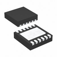
LT3500HDD#TRPBF Linear Technology, LT3500HDD#TRPBF Datasheet - Page 10

LT3500HDD#TRPBF
Manufacturer Part Number
LT3500HDD#TRPBF
Description
IC REG STP-DWN 2A 12-DFN
Manufacturer
Linear Technology
Type
Step-Down (Buck)r
Datasheet
1.LT3500EDDPBF.pdf
(28 pages)
Specifications of LT3500HDD#TRPBF
Topology
Step-Down (Buck) (1), Linear (LDO) (1)
Function
Any Function
Number Of Outputs
2
Frequency - Switching
500kHz ~ 2.4MHz
Voltage/current - Output 1
0.8 ~ 38.9 V, 2A
Voltage/current - Output 2
Adjustable, 13mA
W/led Driver
No
W/supervisor
No
W/sequencer
No
Voltage - Supply
3 V ~ 36 V
Operating Temperature
-40°C ~ 150°C
Mounting Type
Surface Mount
Package / Case
12-DFN
Current - Output
2A
Voltage - Output
0.8 ~ 38.9 V
Voltage - Input
3 ~ 36 V
Internal Switch(s)
Yes
Synchronous Rectifier
No
Lead Free Status / RoHS Status
Lead free / RoHS Compliant
Power - Output
-
Available stocks
Company
Part Number
Manufacturer
Quantity
Price
OPERATION
LT3500
The LT3500 is a constant frequency, current mode buck
converter with an internal 2.3A switch plus a linear regula-
tor with 13mA output capability. Control of both outputs
is achieved with a common SHDN pin, internal regulator,
oscillator, undervoltage detect, soft-start, thermal shut-
down and power-on reset.
If the SHDN pin is taken below its 0.8V threshold, the
LT3500 will be placed in a low quiescent current mode.
In this mode the LT3500 typically draws 12μA from the
V
When the SHDN pin is fl oated or driven above 0.76V, the
internal bias circuits turn on generating an internal regu-
lated voltage, 0.8(V
a POR signal which sets the soft-start latch.
As the R
internal oscillator will start generating a clock signal at a
frequency determined by the resistor from the R
pin to ground. Alternatively, if a synchronization signal is
detected by the LT3500 at the R
will be generated at the incoming frequency on the rising
edge of the synchronization pulse. In addition, the internal
slope compensation will be automatically adjusted to pre-
vent subharmonic oscillation during synchronization.
The LT3500 is a constant frequency, current mode step-
down converter. Current mode regulators are controlled
by an internal clock and two feedback loops that control
the duty cycle of the power switch. In addition to the
normal error amplifi er, there is a current sense amplifi er
that monitors switch current on a cycle-by-cycle basis.
This technique means that the error amplifi er commands
current to be delivered to the output rather than voltage.
A voltage fed system will have low phase shift up to the
resonant frequency of the inductor and output capacitor,
then an abrupt 180° shift will occur. The current fed system
will have 90° phase shift at a much lower frequency, but
will not have the additional 90° shift until well beyond
the LC resonant frequency. This makes it much easier to
frequency compensate the feedback loop and also gives
much quicker transient response.
10
IN
pin.
T
/SYNC pin reaches its 1V regulation point, the
FB
) and 1V(R
T
/SYNC pin, a clock signal
T
/SYNC) references, and
T
/SYNC
During power up, the POR signal sets the soft-start latch,
which discharges the SS pin to ensure proper start-up
operation. When the SS pin voltage drops below 100mV,
the V
start latch is reset. Once the latch is reset the soft-start
capacitor starts to charge with a typical value of 2.75μA.
As the voltage rises above 100mV on the SS pin, the V
pin will be driven high by the error amplifi er. When the
voltage on the V
the driver fl ip-fl op which turns on the internal power NPN
switch. This causes current from V
switch, inductor and internal sense resistor, to increase.
When the voltage drop across the internal sense resistor
exceeds a predetermined level set by the voltage on the
V
is turned off. Once the switch is turned off the inductor
will drive the voltage at the SW pin low until the external
Schottky diode starts to conduct, decreasing the current
in the inductor. The cycle is repeated with the start of each
clock cycle. However, if the internal sense resistor voltage
exceeds the predetermined level at the start of a clock cycle,
the fl ip-fl op will not be set resulting in a further decrease in
inductor current. Since the output current is controlled by
the V
amplifi er continually adjusting the V
The error amplifi er is a transconductance amplifi er that
compares the FB voltage to either the SS pin voltage minus
100mV or an internally regulated 800mV, whichever is
lowest. Compensation of the loop is easily achieved with
a simple capacitor or series resistor/capacitor from the
V
Since the SS pin is driven by a constant current source, a
single capacitor on the soft-start pin will generate controlled
linear ramp on the output voltage.
If the current demanded by the output exceeds the maxi-
mum current dictated by the V
will be discharged, lowering the regulation point until the
output voltage can be supported by the maximum current.
When overload is removed, the output will soft-start from
the overload regulation point.
C
C
pin, the fl ip-fl op is reset and the internal NPN switch
pin to ground.
C
C
pin is driven low disabling switching and the soft-
voltage, output regulation is achieved by the error
C
pin exceeds 0.8V, the clock set-pulse sets
C
pin clamp, the SS pin
IN
C
, through the NPN
pin voltage.
3500fc
C


