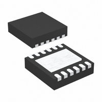
LT3500HDD#TRPBF Linear Technology, LT3500HDD#TRPBF Datasheet - Page 23

LT3500HDD#TRPBF
Manufacturer Part Number
LT3500HDD#TRPBF
Description
IC REG STP-DWN 2A 12-DFN
Manufacturer
Linear Technology
Type
Step-Down (Buck)r
Datasheet
1.LT3500EDDPBF.pdf
(28 pages)
Specifications of LT3500HDD#TRPBF
Topology
Step-Down (Buck) (1), Linear (LDO) (1)
Function
Any Function
Number Of Outputs
2
Frequency - Switching
500kHz ~ 2.4MHz
Voltage/current - Output 1
0.8 ~ 38.9 V, 2A
Voltage/current - Output 2
Adjustable, 13mA
W/led Driver
No
W/supervisor
No
W/sequencer
No
Voltage - Supply
3 V ~ 36 V
Operating Temperature
-40°C ~ 150°C
Mounting Type
Surface Mount
Package / Case
12-DFN
Current - Output
2A
Voltage - Output
0.8 ~ 38.9 V
Voltage - Input
3 ~ 36 V
Internal Switch(s)
Yes
Synchronous Rectifier
No
Lead Free Status / RoHS Status
Lead free / RoHS Compliant
Power - Output
-
Available stocks
Company
Part Number
Manufacturer
Quantity
Price
APPLICATIONS INFORMATION
capacitor C2. Additionally, the SW and BST traces should
be kept as short as possible. The topside metal from the
DC1069A demonstration board in Figure 12 illustrates
proper component placement and trace routing.
Thermal Considerations
The PCB must also provide heat sinking to keep the
LT3500 cool. The exposed metal on the bottom of the
package must be soldered to a ground plane. This ground
Figure 11. Subtracting the Current when the Switch is On (11a) from the Current when the Switch is Off (11b) Reveals the Path of the
High Frequency Switching Current (11c). Keep this Loop Small. The Voltage on the SW and BST Traces will Also be Switched; Keep
These Traces as Short as Possible. Finally, Make Sure the Circuit is Shielded with a Local Ground Plane
Figure 12. LT3500 Demonstration Circuit Board DC1069A
V
IN
LT3500 SW
GND
(11a)
V
IN
LT3500 SW
GND
(11b)
should be tied to other copper layers below with thermal
vias; these layers will spread the heat dissipated by the
LT3500. Place additional vias near the catch diodes. Adding
more copper to the top and bottom layers and tying this
copper to the internal planes with vias can further reduce
thermal resistance. With these steps, the thermal resis-
tance from die (or junction) to ambient can be reduced to
θ
the MSE Package.
Power dissipation within the LT3500 can be estimated
by calculating the total power loss from an effi ciency
measurement and subtracting the catch diode loss. The
die temperature is calculated by multiplying the LT3500
power dissipation by the thermal resistance from junction
to ambient.
The power dissipation in the other power components
such as catch diodes, boost diodes and inductors, cause
additional copper heating and can further increase what
the IC sees as ambient temperature. See the LT1767 data
sheet’s Thermal Considerations section.
Other Linear Technology Publications
Application notes AN19, AN35 and AN44 contain more
detailed descriptions and design information for buck
regulators and other switching regulators. The LT1376
data sheet has a more extensive discussion of output
ripple, loop compensation and stability testing. Design
note DN100 shows how to generate a dual (+ and –) output
supply using a buck regulator.
JA
= 45°C/W for the DD Package, and θ
V
IN
LT3500 SW
GND
(11c)
JA
LT3500
= 45°C/W for
3500 F11
23
3500fc


