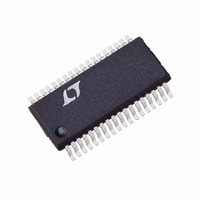
LTC1709EG Linear Technology, LTC1709EG Datasheet - Page 4

LTC1709EG
Manufacturer Part Number
LTC1709EG
Description
IC REG SW 2PH SYNC STPDWN 36SSOP
Manufacturer
Linear Technology
Type
Step-Down (Buck)r
Datasheet
1.LTC1709EG.pdf
(28 pages)
Specifications of LTC1709EG
Internal Switch(s)
No
Synchronous Rectifier
Yes
Number Of Outputs
2
Voltage - Output
1.3 ~ 3.5 V
Current - Output
3A
Voltage - Input
4 ~ 36 V
Operating Temperature
-40°C ~ 85°C
Mounting Type
Surface Mount
Package / Case
36-SSOP
Lead Free Status / RoHS Status
Contains lead / RoHS non-compliant
Power - Output
-
Frequency - Switching
-
Available stocks
Company
Part Number
Manufacturer
Quantity
Price
Company:
Part Number:
LTC1709EG
Manufacturer:
TOSH
Quantity:
3 760
Part Number:
LTC1709EG
Manufacturer:
LT/凌特
Quantity:
20 000
Company:
Part Number:
LTC1709EG-7
Manufacturer:
LT
Quantity:
392
Part Number:
LTC1709EG-7
Manufacturer:
LT/凌特
Quantity:
20 000
Company:
Part Number:
LTC1709EG-7#PBF
Manufacturer:
Linear Technology
Quantity:
135
Part Number:
LTC1709EG-8
Manufacturer:
LT/凌特
Quantity:
20 000
Company:
Part Number:
LTC1709EG-85
Manufacturer:
LT
Quantity:
389
Part Number:
LTC1709EG-85
Manufacturer:
LT/凌特
Quantity:
20 000
Part Number:
LTC1709EG-85#TR
Manufacturer:
LT/凌特
Quantity:
20 000
ELECTRICAL CHARACTERISTICS
LTC1709
temperature range, otherwise specifications are at T
SYMBOL
R
V
I
A
V
CMRR
PSRR
I
V
GBW
SR
Note 1: Absolute Maximum Ratings are those values beyond which the
life of a device may be impaired.
Note 2: The LTC1709EG is guaranteed to meet performance specifications
from 0 C to 70 C. Specifications over the – 40 C to 85 C operating
temperature range are assured by design, characterization and correlation
with statistical process controls.
Note 3: T
dissipation P
LTC1709EG: T
Note 4: The LTC1709 is tested in a feedback loop that servos V
specified voltage and measures the resultant V
Note 5: Dynamic supply current is higher due to the gate charge being
delivered at the switching frequency. See Applications Information.
4
TYPICAL PERFOR A CE CHARACTERISTICS
B
CL
OS
OL
CM
O(MAX)
IN
100
80
60
40
20
0
OA
0.1
OA
Efficiency vs Output Current
(Figure 12)
J
is calculated from the ambient temperature T
D
PARAMETER
Input Resistance
Input Offset Voltage
Input Bias Current
Open Loop DC Gain
Common Mode Input Voltage Range
Common Mode Rejection Ratio
Power Supply Rejection Ratio
Maximum Output Current
Maximum Output Voltage
Gain-Bandwidth Product
Slew Rate
J
according to the following formulas:
= T
OUTPUT CURRENT (A)
A
1
+ (P
D
V
V
V
V
• 85 C/W)
IN
IN
IN
IN
= 5V
= 8V
= 12V
= 20V
10
V
V
f = 200kHz
OUT
EXTVCC
W
= 2V
= 0V
1709 G01
U
100
EAIN
.
A
CONDITIONS
Differential Amp Mode; Measured at V
Op Amp Mode; V
I
Op Amp Mode
Op Amp Mode; 0.7V V
Op Amp Mode
Op Amp Mode; 0V < V
Op Amp Mode; 6V < V
Op Amp Mode; V
Op Amp Mode; I
Op Amp Mode; I
Op Amp Mode; R
100
DIFFOUT
and power
80
60
40
20
0
0.1
A
Efficiency vs Output Current
(Figure 12)
= 25 C. V
ITH
V
V
f = 200kHz
OUT
IN
= 1mA
to a
= 12V
INTERNAL LDO VS EXTERNALLY
APPLIED 5V OVERALL EFFICIENCY
(FIGURE 12)
The
= 2V
OUTPUT CURRENT (A)
DIFFOUT
DIFFOUT
IN
CM
DIFFOUT
1
L
= 2k
denotes the specifications which apply over the full operating
= 15V, V
= 2.5V; V
V
V
EXTVCC
EXTVCC
CM
IN
= 1mA
= 1mA
Note 6: Rise and fall times are measured using 10% and 90% levels. Delay
times are measured using 50% levels.
Note 7: The minimum on-time condition corresponds to the on inductor
peak-to-peak ripple current 40% I
Considerations in the Applications Information section).
Note 8: Each built-in pull-up resistor attached to the VID inputs also has a
series diode to allow input voltages higher than the VIDV
damage or clamping (see the Applications Information section).
Note 9: When the AMPMD pin is high, the IC pins are connected directly to
the internal op amp inputs. When the AMPMD pin is low, internal MOSFET
switches connect four 40k resistors around the op amp to create a
standard unity-gain differential amp.
DIFFOUT
< 30V
= 0V
< 3V
= 5V
= 0V
RUN/SS
DIFFOUT
10
< 10V
= 5V;
= 5V unless otherwise noted.
OS
1709 G02
+ Input
100
100
90
80
70
5
Efficiency vs Input Voltage
(Figure 12)
MAX
V
V
I
OUT
MIN
OUT
EXTVCC
70
70
10
10
0
(see Minimum On-Time
= 20A
= 3.3V
= 5V
10
5000
TYP
80
30
90
90
35
11
2
5
V
IN
(V)
CC
MAX
200
15
supply without
6
3
1709 G03
UNITS
V/mV
MHz
V/ s
mV
mA
k
20
nA
dB
dB
V
V


