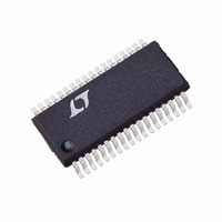
LTC1709EG Linear Technology, LTC1709EG Datasheet - Page 13

LTC1709EG
Manufacturer Part Number
LTC1709EG
Description
IC REG SW 2PH SYNC STPDWN 36SSOP
Manufacturer
Linear Technology
Type
Step-Down (Buck)r
Datasheet
1.LTC1709EG.pdf
(28 pages)
Specifications of LTC1709EG
Internal Switch(s)
No
Synchronous Rectifier
Yes
Number Of Outputs
2
Voltage - Output
1.3 ~ 3.5 V
Current - Output
3A
Voltage - Input
4 ~ 36 V
Operating Temperature
-40°C ~ 85°C
Mounting Type
Surface Mount
Package / Case
36-SSOP
Lead Free Status / RoHS Status
Contains lead / RoHS non-compliant
Power - Output
-
Frequency - Switching
-
Available stocks
Company
Part Number
Manufacturer
Quantity
Price
Company:
Part Number:
LTC1709EG
Manufacturer:
TOSH
Quantity:
3 760
Part Number:
LTC1709EG
Manufacturer:
LT/凌特
Quantity:
20 000
Company:
Part Number:
LTC1709EG-7
Manufacturer:
LT
Quantity:
392
Part Number:
LTC1709EG-7
Manufacturer:
LT/凌特
Quantity:
20 000
Company:
Part Number:
LTC1709EG-7#PBF
Manufacturer:
Linear Technology
Quantity:
135
Part Number:
LTC1709EG-8
Manufacturer:
LT/凌特
Quantity:
20 000
Company:
Part Number:
LTC1709EG-85
Manufacturer:
LT
Quantity:
389
Part Number:
LTC1709EG-85
Manufacturer:
LT/凌特
Quantity:
20 000
Part Number:
LTC1709EG-85#TR
Manufacturer:
LT/凌特
Quantity:
20 000
APPLICATIO S I FOR ATIO
but it is very dependent on inductance selected. As induc-
tance increases, core losses go down. Unfortunately,
increased inductance requires more turns of wire and
therefore copper losses will increase.
Ferrite designs have very low core loss and are preferred
at high switching frequencies, so design goals can con-
centrate on copper loss and preventing saturation. Ferrite
core material saturates “hard,” which means that induc-
tance collapses abruptly when the peak design current is
exceeded. This results in an abrupt increase in inductor
ripple current and consequent output voltage ripple. Do
not allow the core to saturate!
Molypermalloy (from Magnetics, Inc.) is a very good, low
loss core material for toroids, but it is more expensive than
ferrite. A reasonable compromise from the same manu-
facturer is Kool M . Toroids are very space efficient,
especially when you can use several layers of wire. Be-
cause they lack a bobbin, mounting is more difficult.
However, designs for surface mount are available which
do not increase the height significantly.
Power MOSFET, D1 and D2 Selection
Two external power MOSFETs must be selected for each
output stage for the LTC1709: One N-channel MOSFET for
the top (main) switch, and one N-channel MOSFET for the
bottom (synchronous) switch.
The peak-to-peak drive levels are set by the INTV
age. This voltage is typically 5V during start-up (see
EXTV
old MOSFETs must be used in most applications. The only
exception is if low input voltage is expected (V
then, sublogic-level threshold MOSFETs (V
should be used. Pay close attention to the BV
cation for the MOSFETs as well; most of the logic-level
MOSFETs are limited to 30V or less.
Selection criteria for the power MOSFETs include the “ON”
resistance R
input voltage, and maximum output current. When the
LTC1709 is operating in continuous mode the duty factors
for the top and bottom MOSFETs of each output stage are
given by:
CC
Pin Connection). Consequently, logic-level thresh-
DS(ON)
, reverse transfer capacitance C
U
U
W
GS(TH)
DSS
U
IN
CC
specifi-
< 5V);
< 1V)
volt-
RSS
,
The MOSFET power dissipations at maximum output
current are given by:
where is the temperature dependency of R
is a constant inversely related to the gate drive current.
Both MOSFETs have I
equation includes an additional term for transition losses,
which peak at the highest input voltage. For V
high current efficiency generally improves with larger
MOSFETs, while for V
increase to the point that the use of a higher R
with lower C
synchronous MOSFET losses are greatest at high input
voltage when the top switch duty factor is low or during a
short-circuit when the synchronous switch is on close to
100% of the period.
The term (1 + ) is generally given for a MOSFET in the
form of a normalized R
voltage MOSFETs. C
FET characteristics. The constant k = 1.7 can be used to
estimate the contributions of the two terms in the main
switch dissipation equation.
The Schottky diodes, D1 and D2 shown in Figure 1 conduct
during the dead-time between the conduction of the two
large power MOSFETs. This helps prevent the body diode
= 0.005/ C can be used as an approximation for low
Main Switch Duty Cycle
P
P
Synchronous Switch Duty Cycle
MAIN
SYNC
k V
V
V
V
OUT
IN
RSS
IN
IN
–
V
2
IN
actual provides higher efficiency. The
V
I
I
OUT
MAX
MAX
RSS
2
2
2
IN
R losses but the topside N-channel
DS(ON)
> 20V the transition losses rapidly
is usually specified in the MOS-
I
2
MAX
C
2
1
RSS
vs. Temperature curve, but
V
V
2
OUT
IN
R
1
f
DS ON
(
R
LTC1709
V
)
DS ON
IN
(
DS(ON)
–
V
DS(ON)
IN
IN
V
)
< 20V the
OUT
13
device
and k


