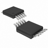
LTC1871IMS Linear Technology, LTC1871IMS Datasheet - Page 27

LTC1871IMS
Manufacturer Part Number
LTC1871IMS
Description
IC MULTI CONFIG SYNC ADJ 10MSOP
Manufacturer
Linear Technology
Type
Step-Up (Boost), Flyback, Sepicr
Datasheet
1.LTC1871EMS.pdf
(36 pages)
Specifications of LTC1871IMS
Internal Switch(s)
No
Synchronous Rectifier
No
Number Of Outputs
1
Voltage - Output
1.23 ~ 72 V
Current - Output
50mA
Frequency - Switching
50kHz ~ 1MHz
Voltage - Input
2.5 ~ 36 V
Operating Temperature
-40°C ~ 125°C
Mounting Type
Surface Mount
Package / Case
10-MSOP, Micro10™, 10-uMAX, 10-uSOP
Lead Free Status / RoHS Status
Contains lead / RoHS non-compliant
Power - Output
-
Available stocks
Company
Part Number
Manufacturer
Quantity
Price
Company:
Part Number:
LTC1871IMS
Manufacturer:
LT
Quantity:
10 000
Part Number:
LTC1871IMS
Manufacturer:
LINEAR
Quantity:
20 000
Company:
Part Number:
LTC1871IMS#3CFPBF
Manufacturer:
LT
Quantity:
2 043
Company:
Part Number:
LTC1871IMS#PBF
Manufacturer:
LT
Quantity:
2 058
Company:
Part Number:
LTC1871IMS-1
Manufacturer:
LT
Quantity:
10 000
Company:
Part Number:
LTC1871IMS-7
Manufacturer:
LT
Quantity:
10 000
APPLICATIONS INFORMATION
SEPIC Converter: Output Capacitor Selection
Because of the improved performance of today’s electro-
lytic, tantalum and ceramic capacitors, engineers need
to consider the contributions of ESR (equivalent series
resistance), ESL (equivalent series inductance) and the
bulk capacitance when choosing the correct component
for a given output ripple voltage. The effects of these three
parameters (ESR, ESL, and bulk C) on the output voltage
ripple waveform are illustrated in Figure 17 for a typical
coupled-inductor SEPIC converter.
Figure 17. SEPIC Converter Switching Waveforms
V
17c. DC Coupling Capacitor Current
(AC)
OUT
I
I
I
I
C1
D1
L1
L2
17b. Output Inductor Current
17a. Input Inductor Current
17e. Output Ripple Voltage
SW
ON
17d. Diode Current
ΔV
OFF
SW
ESR
RINGING DUE TO
TOTAL INDUCTANCE
(BOARD + CAP)
ΔV
COUT
I
I
I
I
I
IN
O
IN
O
O
The choice of component(s) begins with the maximum
acceptable ripple voltage (expressed as a percentage of
the output voltage), and how this ripple should be divided
between the ESR step and the charging/discharging ΔV.
For the purpose of simplicity we will choose 2% for the
maximum output ripple, to be divided equally between the
ESR step and the charging/discharging ΔV. This percentage
ripple will change, depending on the requirements of the
application, and the equations provided below can easily
be modifi ed.
For a 1% contribution to the total ripple voltage, the ESR
of the output capacitor can be determined using the fol-
lowing equation:
where:
For the bulk C component, which also contributes 1% to
the total ripple:
For many designs it is possible to choose a single capacitor
type that satisfi es both the ESR and bulk C requirements
for the design. In certain demanding applications, however,
the ripple voltage can be improved signifi cantly by con-
necting two or more types of capacitors in parallel. For
example, using a low ESR ceramic capacitor can minimize
the ESR step, while an electrolytic or tantalum capacitor
can be used to supply the required bulk C.
Once the output capacitor ESR and bulk capacitance have
been determined, the overall ripple voltage waveform
should be verifi ed on a dedicated PC board (see Board
Layout section for more information on component place-
ment). Lab breadboards generally suffer from excessive
series inductance (due to inter-component wiring), and
these parasitics can make the switching waveforms look
signifi cantly worse than they would be on a properly
designed PC board.
ESR
I
C
D(PEAK)
OUT
COUT
0.01• V
= 1+
I
O(MAX)
0.01• V
I
D(PEAK)
2
O
• f
•I
O
O(MAX)
•
V
V
IN(MIN)
O
+ V
LTC1871
D
+ 1
27
1871fe


