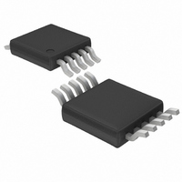
LTC1871IMS Linear Technology, LTC1871IMS Datasheet - Page 18

LTC1871IMS
Manufacturer Part Number
LTC1871IMS
Description
IC MULTI CONFIG SYNC ADJ 10MSOP
Manufacturer
Linear Technology
Type
Step-Up (Boost), Flyback, Sepicr
Datasheet
1.LTC1871EMS.pdf
(36 pages)
Specifications of LTC1871IMS
Internal Switch(s)
No
Synchronous Rectifier
No
Number Of Outputs
1
Voltage - Output
1.23 ~ 72 V
Current - Output
50mA
Frequency - Switching
50kHz ~ 1MHz
Voltage - Input
2.5 ~ 36 V
Operating Temperature
-40°C ~ 125°C
Mounting Type
Surface Mount
Package / Case
10-MSOP, Micro10™, 10-uMAX, 10-uSOP
Lead Free Status / RoHS Status
Contains lead / RoHS non-compliant
Power - Output
-
Available stocks
Company
Part Number
Manufacturer
Quantity
Price
Company:
Part Number:
LTC1871IMS
Manufacturer:
LT
Quantity:
10 000
Part Number:
LTC1871IMS
Manufacturer:
LINEAR
Quantity:
20 000
Company:
Part Number:
LTC1871IMS#3CFPBF
Manufacturer:
LT
Quantity:
2 043
Company:
Part Number:
LTC1871IMS#PBF
Manufacturer:
LT
Quantity:
2 058
Company:
Part Number:
LTC1871IMS-1
Manufacturer:
LT
Quantity:
10 000
Company:
Part Number:
LTC1871IMS-7
Manufacturer:
LT
Quantity:
10 000
LTC1871
APPLICATIONS INFORMATION
Boost Converter: Input Capacitor Selection
The input capacitor of a boost converter is less critical
than the output capacitor, due to the fact that the inductor
is in series with the input and the input current waveform
is continuous (see Figure 12b). The input voltage source
impedance determines the size of the input capacitor,
which is typically in the range of 10μF to 100μF . A low ESR
capacitor is recommended, although it is not as critical as
for the output capacitor.
The RMS input capacitor ripple current for a boost con-
verter is:
18
I
RMS(CIN)
Figure 12. Switching Waveforms for a Boost Converter
12e. Output Voltage Ripple Waveform
V
(AC)
I
OUT
SW
12b. Inductor and Input Currents
I
I
12d. Diode and Output Currents
D
L
V
= 0.3 •
IN
t
ON
12a. Circuit Diagram
12c. Switch Current
L
SW
ΔV
V
t
IN(MIN)
OFF
L • f
ESR
ΔV
D
COUT
• D
MAX
C
OUT
RINGING DUE TO
TOTAL INDUCTANCE
(BOARD + CAP)
V
OUT
I
IN
R
L
I
O
Please note that the input capacitor can see a very high
surge current when a battery is suddenly connected to
the input of the converter and solid tantalum capacitors
can fail catastrophically under these conditions. Be sure
to specify surge-tested capacitors!
Burst Mode Operation and Considerations
The choice of MOSFET R
determines the load current at which the LTC1871 enters
Burst Mode operation. When bursting, the controller
clamps the peak inductor current to approximately:
which represents about 20% of the maximum 150mV
SENSE pin voltage. The corresponding average current
depends upon the amount of ripple current. Lower inductor
values (higher ΔI
Burst Mode operations begins, since it is the peak current
that is being clamped.
The output voltage ripple can increase during Burst Mode
operation if ΔI
occur if the input voltage is very low or if a very large
inductor is chosen. At high duty cycles, a skipped cycle
causes the inductor current to quickly decay to zero.
However, because ΔI
for the current to ramp back up to I
ing this inductor charging interval, the output capacitor
must supply the load current and a signifi cant droop in
the output voltage can occur. Generally, it is a good idea
to choose a value of inductor ΔI
of I
of the output capacitor or disable Burst Mode operation
using the MODE/SYNC pin.
Burst Mode operation can be defeated by connecting the
MODE/SYNC pin to a high logic-level voltage (either with
a control input or by connecting this pin to INTV
this mode, the burst clamp is removed, and the chip can
operate at constant frequency from continuous conduction
mode (CCM) at full load, down into deep discontinuous
conduction mode (DCM) at light load. Prior to skipping
pulses at very light load (i.e., < 5% of full load), the control-
ler will operate with a minimum switch on-time in DCM.
I
BURST(PEAK)
IN(MAX)
. The alternative is to either increase the value
L
is substantially less than I
=
L
R
) will reduce the load current at which
30mV
DS(ON)
L
is small, it takes multiple cycles
DS(ON)
L
and inductor value also
between 25% and 40%
BURST(PEAK)
BURST
. This can
CC
. Dur-
). In
1871fe


