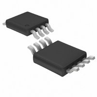
LTC1877EMS8#TR Linear Technology, LTC1877EMS8#TR Datasheet - Page 8

LTC1877EMS8#TR
Manufacturer Part Number
LTC1877EMS8#TR
Description
IC BUCK SYNC ADJ .6A 8MSOP
Manufacturer
Linear Technology
Type
Step-Down (Buck)r
Datasheet
1.LTC1877EMS8PBF.pdf
(16 pages)
Specifications of LTC1877EMS8#TR
Internal Switch(s)
Yes
Synchronous Rectifier
Yes
Number Of Outputs
1
Voltage - Output
0.8 ~ 10 V
Current - Output
600mA
Frequency - Switching
550kHz
Voltage - Input
2.65 ~ 10 V
Operating Temperature
-40°C ~ 85°C
Mounting Type
Surface Mount
Package / Case
8-MSOP, Micro8™, 8-uMAX, 8-uSOP,
Lead Free Status / RoHS Status
Contains lead / RoHS non-compliant
Power - Output
-
Available stocks
Company
Part Number
Manufacturer
Quantity
Price
OPERATION
APPLICATIONS INFORMATION
LTC1877
Dropout Operation
When the input supply voltage decreases toward the output
voltage, the duty cycle increases toward the maximum
on-time. Further reduction of the supply voltage forces the
main switch to remain on for more than one cycle until it
reaches 100% duty cycle. The output voltage will then be
determined by the input voltage minus the voltage drop
across the internal P-channel MOSFET and the inductor.
Low Supply Operation
The LTC1877 is designed to operate down to an input supply
voltage of 2.65V although the maximum allowable output
current is reduced at this low voltage. Figure 1 shows the
reduction in the maximum output current as a function of
input voltage for various output voltages.
The basic LTC1877 application circuit is shown on the fi rst
page. External component selection is driven by the load
requirement and begins with the selection of L followed
by C
Inductor Value Calculation
The inductor selection will depend on the operating fre-
quency of the LTC1877. The internal nominal frequency is
550kHz, but can be externally synchronized from 400kHz
to 700kHz.
8
IN
Figure 1. Maximum Output Current vs Input Voltage
and C
1200
1000
OUT
800
600
400
200
0
0
.
2
V
OUT
V
4
= 1.5V
OUT
V IN (V)
= 3.3V
6
V
V
OUT
OUT
8
= 5V
= 2.5V
L = 10μH
10
1877 F01
12
The operating frequency and inductor selection are inter-
related in that higher operating frequencies allow the use of
smaller inductor and capacitor values. However, operating
at a higher frequency generally results in lower effi ciency
because of increased internal gate charge losses.
The inductor value has a direct effect on ripple current.
The ripple current ΔI
or frequency and increases with higher V
Another important detail to remember is that at low input
supply voltages, the R
creases. Therefore, the user should calculate the power
dissipation when the LTC1877 is used at 100% duty cycle
with a low input voltage (see Thermal Considerations in
the Applications Information section).
Slope Compensation and Inductor Peak Current
Slope compensation provides stability in constant-fre-
quency architectures by preventing subharmonic oscilla-
tions at high duty cycles. It is accomplished internally by
adding a compensating ramp to the inductor current signal
at duty cycles in excess of 40%. As a result, the maximum
inductor peak current is reduced for duty cycles >40%.
This is shown in the decrease of the inductor peak current
as a function of duty cycle graph in Figure 2.
Δ =
Figure 2. Maximum Inductor Peak Current vs Duty Cycle
I
L
( )( )
f L
1100
1000
1
900
800
700
600
0
V
V
IN
OUT
= 5V
20
L
⎛
⎜
⎝
1
DS(ON)
decreases with higher inductance
DUTY CYCLE (%)
−
40
V
V
OUT
IN
of the P-channel switch in-
60
⎞
⎟
⎠
80
1877 F02
100
IN
or V
OUT
.
1877fa
(1)


