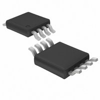
LTC1877EMS8#TR Linear Technology, LTC1877EMS8#TR Datasheet - Page 6

LTC1877EMS8#TR
Manufacturer Part Number
LTC1877EMS8#TR
Description
IC BUCK SYNC ADJ .6A 8MSOP
Manufacturer
Linear Technology
Type
Step-Down (Buck)r
Datasheet
1.LTC1877EMS8PBF.pdf
(16 pages)
Specifications of LTC1877EMS8#TR
Internal Switch(s)
Yes
Synchronous Rectifier
Yes
Number Of Outputs
1
Voltage - Output
0.8 ~ 10 V
Current - Output
600mA
Frequency - Switching
550kHz
Voltage - Input
2.65 ~ 10 V
Operating Temperature
-40°C ~ 85°C
Mounting Type
Surface Mount
Package / Case
8-MSOP, Micro8™, 8-uMAX, 8-uSOP,
Lead Free Status / RoHS Status
Contains lead / RoHS non-compliant
Power - Output
-
Available stocks
Company
Part Number
Manufacturer
Quantity
Price
PIN FUNCTIONS
LTC1877
RUN (Pin 1): Run Control Input. Forcing this pin below
0.4V shuts down the LTC1877. In shutdown, all functions
are disabled drawing <1μA supply current. Forcing this
pin above 1.2V enables the LTC1877. Do not leave RUN
fl oating.
I
comparator threshold increases with this control voltage.
Nominal voltage range for this pin is from 0.5V to 1.9V.
V
from an external resistive divider across the output.
GND (Pin 4): Ground Pin.
SW (Pin 5): Switch Node Connection to Inductor. This pin
connects to the drains of the internal main and synchronous
power MOSFET switches.
FUNCTIONAL DIAGRAM
6
SYNC/MODE
TH
FB
PLL LPF
RUN
(Pin 2): Error Amplifi er Compensation Point. The current
V
1
(Pin 3): Feedback Pin. Receives the feedback voltage
8
7
3
FB
0.6V
+
–
DEFEAT
BURST
0.8V REF
V
IN
SHUTDOWN
X
Y
0.85V
SHIFT
FREQ
VCO
Y = “0” ONLY WHEN X IS A CONSTANT “1”
V
0.8V
REF
g
m
+
–
OVDET
= 0.5m
+
–
EA
SLOPE
COMP
V
–
+
IN
SLEEP
OSC
V
IN
2
0.55V
I
TH
V
to GND, Pin 4.
SYNC/MODE (Pin 7): External Clock Synchronization
and Mode Select Input. To synchronize with an external
clock, apply a clock with a frequency between 400kHz
and 700kHz. To select Burst Mode operation, tie to V
Grounding this pin selects pulse-skipping mode. Do not
leave this pin fl oating.
PLL LPF (Pin 8): Output of the Phase Detector and Control
Input of Oscillator. Connect a series RC lowpass network
from this pin to ground if externally synchronized. If un-
used, this pin may be left open.
IN
RS LATCH
–
+
R
S
(Pin 6): Main Supply Pin. Must be closely decoupled
BURST
EN
Q
Q
SLEEP
SWITCHING
BLANKING
CIRCUIT
LOGIC
AND
0.8V
–
I
SHOOT-
COMP
THRU
ANTI
I
RCMP
+
V
+
–
IN
6Ω
6
5
4
1877fa
1877 BD
V
SW
GND
IN
IN
.


