LT1776CS8#TR Linear Technology, LT1776CS8#TR Datasheet - Page 12

LT1776CS8#TR
Manufacturer Part Number
LT1776CS8#TR
Description
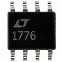
IC REG SW STEPDOWN HI EFF 8SOIC
Manufacturer
Linear Technology
Type
Step-Down (Buck)r
Datasheet
1.LT1776CS8PBF.pdf
(20 pages)
Specifications of LT1776CS8#TR
Internal Switch(s)
Yes
Synchronous Rectifier
No
Number Of Outputs
1
Voltage - Output
1.24 ~ 34 V
Current - Output
700mA
Frequency - Switching
200kHz
Voltage - Input
7.4 ~ 40 V
Operating Temperature
0°C ~ 125°C
Mounting Type
Surface Mount
Package / Case
8-SOIC (3.9mm Width)
Lead Free Status / RoHS Status
Contains lead / RoHS non-compliant
Power - Output
-
Available stocks
Company
Part Number
Manufacturer
Quantity
Price
APPLICATIONS
LT1776
12
However, remember that oscillator slowdown to achieve
short-circuit protection (discussed above) is dependent
on FB pin behavior, and this in turn, is sensitive to FB node
external impedance. Figure 2 shows the typical relation-
ship between FB divider Thevenin voltage and impedance,
and oscillator frequency. This shows that as feedback
network impedance increases beyond 10k, complete os-
cillator slowdown is not achieved, and short-circuit pro-
tection may be compromised. And as a practical matter,
the product of FB pin bias current and larger FB network
impedances will cause increasing output voltage error.
(Nominal cancellation for 10k of FB Thevenin impedance
is included internally.)
Thermal Considerations
Care should be taken to ensure that the worst-case input
voltage and load current conditions do not cause exces-
sive die temperatures. The packages are rated at 110 C/W
for the 8-pin SO (S8) and 130 C/W for 8-pin PDIP (N8).
Quiescent power is given by:
(This assumes that the V
Power loss internal to the LT1776 related to actual output
current is composed of both DC and AC switching losses.
These can be roughly estimated as follows:
DC switching losses are dominated by output switch “ON
voltage”, i.e.,
AC switching losses are typically dominated by power lost
due to the finite rise time and fall time at the V
Assuming, for simplicity, a linear ramp up of both voltage
and current and a current rise/fall time equal to 15ns,
P
P
V
I
DC = ON duty cycle
OUT
Q
DC
ON
= I
= Output switch ON voltage, typically 1V at 500mA
= V
= Output current
IN
ON
• V
• I
IN
OUT
+ I
U
VCC
• DC
• V
INFORMATION
CC
U
OUT
pin is connected to V
W
U
SW
OUT
node.
.)
Total power dissipation of the die is simply the sum of
quiescent, DC and AC losses previously calculated.
Frequency Compensation
Loop frequency compensation is performed by connect-
ing a capacitor, or in most cases a series RC, from the
output of the error amplifier (V
loop compensation may be obtained by empirical meth-
ods as described in detail in Application Note 19. Briefly,
this involves applying a load transient and observing the
dynamic response over the expected range of V
I
As a practical matter, a second small capacitor, directly
from the V
attenuate capacitive coupling from the V
value for this capacitor is 100pF. (See Switch Node Con-
siderations).
Switch Node Considerations
For maximum efficiency, switch rise and fall times are
made as short as practical. To prevent radiation and high
frequency resonance problems, proper layout of the com-
ponents connected to the IC is essential, especially the
power path. B field (magnetic) radiation is minimized by
keeping output diode, switch pin and input bypass capaci-
tor leads as short as possible. E field radiation is kept low
by minimizing the length and area of all traces connected
to the switch pin (V
used under the switcher circuitry to prevent interplane
coupling.
LOAD
P
t
t
f = switching frequency
P
r
f
AC
D(TOTAL)
= (V
= (V
values.
(V
= 1/2 • V
IN
IN
IN
/0.16)ns in low dV/dt mode
/1.6)ns (irrespective of dV/dt mode)
/1.6)ns in high dV/dt mode
C
pin to ground is generally recommended to
= P
IN
Q
+ P
• I
SW
OUT
DC
). A ground plane should always be
• (t
+ P
r
AC
+ t
f
C
+ 30ns) • f
pin) to ground. Proper
SW
pin. A typical
IN
and


