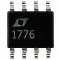
LT1776CS8#TR Linear Technology, LT1776CS8#TR Datasheet - Page 11

LT1776CS8#TR
Manufacturer Part Number
LT1776CS8#TR
Description
IC REG SW STEPDOWN HI EFF 8SOIC
Manufacturer
Linear Technology
Type
Step-Down (Buck)r
Datasheet
1.LT1776CS8PBF.pdf
(20 pages)
Specifications of LT1776CS8#TR
Internal Switch(s)
Yes
Synchronous Rectifier
No
Number Of Outputs
1
Voltage - Output
1.24 ~ 34 V
Current - Output
700mA
Frequency - Switching
200kHz
Voltage - Input
7.4 ~ 40 V
Operating Temperature
0°C ~ 125°C
Mounting Type
Surface Mount
Package / Case
8-SOIC (3.9mm Width)
Lead Free Status / RoHS Status
Contains lead / RoHS non-compliant
Power - Output
-
Available stocks
Company
Part Number
Manufacturer
Quantity
Price
APPLICATIONS
output controls the shutdown pin allows high efficiency at
light loads through Burst Mode operation behavior (see
Typical Applications and Figure 8).
Maximum Load/Short-Circuit Considerations
The LT1776 is a current mode controller. It uses the V
node voltage as an input to a current comparator which
turns off the output switch on a cycle-by-cycle basis as
this peak current is reached. The internal clamp on the V
node, nominally 2V, then acts as an output switch peak
current limit. This action becomes the switch current limit
specification. The maximum available output power is
then determined by the switch current limit.
A potential controllability problem could occur under
short-circuit conditions. If the power supply output is
short circuited, the feedback amplifier responds to the low
output voltage by raising the control voltage, V
peak current limit value. Ideally, the output switch would
be turned on, and then turned off as its current exceeded
the value indicated by V
time involved in both the current comparator and turnoff
of the output switch. These result in a minimum ON time
t
(V
voltage drop, the potential exists for a loss of control.
Expressed mathematically the requirement to maintain
control is:
where:
f = switching frequency
t
V
V
I • R = inductor I • R voltage drop
If this condition is not observed, the current will not be
limited at I
higher value. Using the nominal LT1776 clock frequency
of 200KHz, a V
maximum t
90ns, an unacceptably short time.
ON(MIN)
ON
F
IN
F
f t
= diode forward voltage
+ I • R), the diode forward voltage plus inductor I • R
= switch ON time
= Input voltage
•
ON
. When combined with the large ratio of V
PK
ON
V
, but will cycle-by-cycle ratchet up to some
F
to maintain control would be approximately
IN
V
IN
of 40V and a (V
I R
•
U
C
. However, there is finite response
INFORMATION
U
F
+ I • R) of say 0.7V, the
W
U
C
, to its
IN
to
C
C
The solution to this dilemma is to slow down the oscillator
when the FB pin voltage is abnormally low thereby indicat-
ing some sort of short-circuit condition. Figure 2 shows
the typical response of Oscillator Frequency vs FB divider
Thevenin voltage and impedance. Oscillator frequency is
unaffected until FB voltage drops to about 2/3 of its normal
value. Below this point the oscillator frequency decreases
roughly linearly down to a limit of about 30kHz. This lower
oscillator frequency during short-circuit conditions can
then maintain control with the effective minimum ON time.
A further potential problem with short-circuit operation
might occur if the user were operating the part with its
oscillator slaved to an external frequency source via the
SYNC pin. However, the LT1776 has circuitry that auto-
matically disables the sync function when the oscillator is
slowed down due to abnormally low FB voltage.
Feedback Divider Considerations
An LT1776 application typically includes a resistive divider
between V
the FB pin to the reference voltage V
a fixed ratio between the two resistors, but a second
degree of freedom is offered by the overall impedance level
of the resistor pair. The most obvious effect this has is one
of efficiency—a higher resistance feedback divider will
waste less power and offer somewhat higher efficiency,
especially at light load.
Figure 2. Oscillator Frequency vs FB Divider
Thevenin Voltage and Impedance
OUT
200
150
100
50
0
0
and ground, the center node of which drives
R
TH
FB DIVIDER THEVENIN VOLTAGE (V)
= 10k
0.25
R
TH
= 22k
0.50
R
TH
0.75
= 4.7k
R
TH
FB
1.00
REF
LT1776
. This establishes
1776 F02
1.25
LT1776
11


