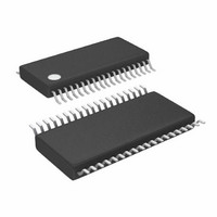
LTC3865EFE#PBF Linear Technology, LTC3865EFE#PBF Datasheet - Page 26

LTC3865EFE#PBF
Manufacturer Part Number
LTC3865EFE#PBF
Description
IC BUCK SYNC ADJ DUAL 38TSSOP
Manufacturer
Linear Technology
Type
Step-Down (Buck)r
Datasheet
1.LTC3865EUHPBF.pdf
(38 pages)
Specifications of LTC3865EFE#PBF
Internal Switch(s)
No
Synchronous Rectifier
Yes
Number Of Outputs
2
Voltage - Output
0.6 ~ 5 V
Frequency - Switching
250kHz ~ 770kHz
Voltage - Input
4.5 ~ 38 V
Operating Temperature
-40°C ~ 85°C
Mounting Type
Surface Mount
Package / Case
38-TSSOP Exposed Pad, 38-eTSSOP, 38-HTSSOP
Primary Input Voltage
15V
No. Of Outputs
2
Output Voltage
5V
Output Current
25A
No. Of Pins
38
Operating Temperature Range
-40°C To +85°C
Msl
MSL 1 - Unlimited
Rohs Compliant
Yes
Lead Free Status / RoHS Status
Lead free / RoHS Compliant
Current - Output
-
Power - Output
-
Available stocks
Company
Part Number
Manufacturer
Quantity
Price
LTC3865/LTC3865-1
APPLICATIONS INFORMATION
Other “hidden” losses such as copper trace and internal
battery resistances can account for an additional 5% to
10% effi ciency degradation in portable systems. It is
26
3. I
4. Transition losses apply only to the topside MOSFET(s),
Supplying INTV
output-derived source will scale the V
quired for the driver and control circuits by a factor
of (Duty Cycle)/(Effi ciency). For example, in a 20V
to 5V application, 10mA of INTV
approximately 2.5mA of V
mid-current loss from 10% or more (if the driver was
powered directly from V
fuse (if used), MOSFET, inductor, current sense resistor.
In continuous mode, the average output current fl ows
through L and R
topside MOSFET and the synchronous MOSFET. If the
two MOSFETs have approximately the same R
then the resistance of one MOSFET can simply be
summed with the resistances of L and R
I
10mΩ, R
25mΩ. This results in losses ranging from 2% to 8%
as the output current increases from 3A to 15A for
a 5V output, or a 3% to 12% loss for a 3.3V output.
Effi ciency varies as the inverse square of V
same external components and output power level. The
combined effects of increasingly lower output voltages
and higher currents required by high performance digital
systems is not doubling but quadrupling the importance
of loss terms in the switching regulator system!
and become signifi cant only when operating at high
input voltages (typically 15V or greater). Transition
losses can be estimated from:
2
2
R losses are predicted from the DC resistances of the
R losses. For example, if each R
Transition Loss = (1.7) V
SENSE
CC
= 5mΩ, then the total resistance is
SENSE
power through EXTV
, but is “chopped” between the
IN
) to only a few percent.
IN
IN
current. This reduces the
2
I
O(MAX)
CC
DS(ON)
current results in
C
SENSE
IN
= 10mΩ, R
RSS
CC
current re-
OUT
f
to obtain
from an
DS(ON)
for the
L
=
,
very important to include these “system” level losses
during the design phase. The internal battery and fuse
resistance losses can be minimized by making sure that
C
switching frequency. A 25W supply will typically require a
minimum of 20μF to 40μF of capacitance having a max-
imum of 20mΩ to 50mΩ of ESR. The LTC3865 2-phase
architecture typically halves this input capacitance require-
ment over competing solutions. Other losses including
Schottky conduction losses during dead time and induc-
tor core losses generally account for less than 2% total
additional loss.
Checking Transient Response
The regulator loop response can be checked by looking at
the load current transient response. Switching regulators
take several cycles to respond to a step in DC (resistive)
load current. When a load step occurs, V
amount equal to ΔI
series resistance of C
discharge C
forces the regulator to adapt to the current change and
return V
time V
ringing, which would indicate a stability problem. The
availability of the I
control loop behavior but also provides a DC coupled and
AC fi ltered closed loop response test point. The DC step,
rise time and settling at this test point truly refl ects the
closed loop response. Assuming a predominantly second
order system, phase margin and/or damping factor can be
estimated using the percentage of overshoot seen at this
pin. The bandwidth can also be estimated by examining the
rise time at the pin. The I
in the Typical Application circuit will provide an adequate
starting point for most applications.
IN
has adequate charge storage and very low ESR at the
OUT
OUT
can be monitored for excessive overshoot or
OUT
to its steady-state value. During this recovery
generating the feedback error signal that
TH
LOAD
OUT
pin not only allows optimization of
(ESR), where ESR is the effective
. ΔI
TH
LOAD
external components shown
also begins to charge or
OUT
shifts by an
3865fb


