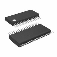
LTC3865EFE#PBF Linear Technology, LTC3865EFE#PBF Datasheet - Page 18

LTC3865EFE#PBF
Manufacturer Part Number
LTC3865EFE#PBF
Description
IC BUCK SYNC ADJ DUAL 38TSSOP
Manufacturer
Linear Technology
Type
Step-Down (Buck)r
Datasheet
1.LTC3865EUHPBF.pdf
(38 pages)
Specifications of LTC3865EFE#PBF
Internal Switch(s)
No
Synchronous Rectifier
Yes
Number Of Outputs
2
Voltage - Output
0.6 ~ 5 V
Frequency - Switching
250kHz ~ 770kHz
Voltage - Input
4.5 ~ 38 V
Operating Temperature
-40°C ~ 85°C
Mounting Type
Surface Mount
Package / Case
38-TSSOP Exposed Pad, 38-eTSSOP, 38-HTSSOP
Primary Input Voltage
15V
No. Of Outputs
2
Output Voltage
5V
Output Current
25A
No. Of Pins
38
Operating Temperature Range
-40°C To +85°C
Msl
MSL 1 - Unlimited
Rohs Compliant
Yes
Lead Free Status / RoHS Status
Lead free / RoHS Compliant
Current - Output
-
Power - Output
-
Available stocks
Company
Part Number
Manufacturer
Quantity
Price
LTC3865/LTC3865-1
APPLICATIONS INFORMATION
Lower ripple current reduces core losses in the inductor,
ESR losses in the output capacitors, and output voltage
ripple. Thus, highest effi ciency operation is obtained at
low frequency with a small ripple current. Achieving this,
however, requires a large inductor.
A reasonable starting point is to choose a ripple current
that is about 40% of I
current occurs at the highest input voltage. To guarantee
that ripple current does not exceed a specifi ed maximum,
the inductor should be chosen according to:
Inductor Core Selection
Once the inductance value is determined, the type of in-
ductor must be selected. Core loss is independent of core
size for a fi xed inductor value, but it is very dependent
on inductance selected. As inductance increases, core
losses go down. Unfortunately, increased inductance
requires more turns of wire and therefore copper losses
will increase.
Ferrite designs have very low core loss and are preferred
at high switching frequencies, so design goals can con-
centrate on copper loss and preventing saturation. Ferrite
core material saturates “hard,” which means that induc-
tance collapses abruptly when the peak design current is
exceeded. This results in an abrupt increase in inductor
ripple current and consequent output voltage ripple. Do
not allow the core to saturate!
Power MOSFET and Schottky Diode
(Optional) Selection
Two external power MOSFETs must be selected for each
controller in the LTC3865/LTC3865-1: one N-channel
MOSFET for the top (main) switch, and one N-channel
MOSFET for the bottom (synchronous) switch.
The peak-to-peak drive levels are set by the INTV
voltage. This voltage is typically 5V during start-up
(see EXTV
threshold MOSFETs must be used in most applications.
The only exception is if low input voltage is expected
18
L
≥
f
OSC RIPPLE
V
IN
CC
–
•
I
V
Pin Connection). Consequently, logic-level
OUT
•
OUT(MAX)
V
V
OUT
IN
. Note that the largest ripple
CC
(V
(V
BV
logic-level MOSFETs are limited to 30V or less.
Selection criteria for the power MOSFETs include the on-
resistance, R
voltage and maximum output current. Miller capacitance,
C
usually provided on the MOSFET manufacturers’ data
sheet. C
along the horizontal axis while the curve is approximately
fl at divided by the specifi ed change in V
then multiplied by the ratio of the application applied V
to the gate charge curve specifi ed V
operating in continuous mode the duty cycles for the top
and bottom MOSFETs are given by:
The MOSFET power dissipations at maximum output
current are given by:
where δ is the temperature dependency of R
R
at the MOSFET’s Miller threshold voltage. V
typical MOSFET minimum threshold voltage.
Both MOSFETs have I
equation includes an additional term for transition losses,
MILLER
DR
IN
GS(TH)
DSS
Main Switch Duty Cycle
P
Synchronous Switc
P
SYNC
MAIN
(approximately 2Ω) is the effective driver resistance
< 5V); then, sub-logic level threshold MOSFETs
specifi cation for the MOSFETs as well; most of the
, can be approximated from the gate charge curve
MILLER
< 3V) should be used. Pay close attention to the
=
=
⎡
⎢
⎢
⎣
( )
V
V
V
V
IN
INTVCC
V
IN
OUT
DS(ON)
IN
–
2
V
is equal to the increase in gate charge
IN
⎛
⎜
⎝
(
V
I
I
OUT
MAX
MAX
–
, Miller capacitance, C
2 2
1
2
V
R losses while the topside N-channel
TH MIN
(
h h Duty Cycle
)
⎞
⎟
⎠
I
2
MAX
(
R
(
(
1 δ
=
DR
+
) )
V
)
2
)(
V
OUT
+
)
(
IN
R
C
1 δ R
V
MILLER
+
DS ON
T T H MIN
=
(
(
)
1
DS
V
)
DS ON
IN
. When the IC is
DS
+
)
)
(
•
–
⎤
⎥
⎥
⎦
V
. This result is
•
IN
MILLER
TH(MIN)
V
f
)
OUT
OSC
DS(ON)
, input
is the
3865fb
and
DS


