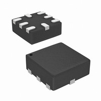
SC195ULTRT Semtech, SC195ULTRT Datasheet - Page 17

SC195ULTRT
Manufacturer Part Number
SC195ULTRT
Description
IC BUCK ADJ .5A 8-MLPQ
Manufacturer
Semtech
Type
Step-Down (Buck)r
Datasheet
1.SC195ULTRT.pdf
(20 pages)
Specifications of SC195ULTRT
Internal Switch(s)
Yes
Synchronous Rectifier
Yes
Number Of Outputs
1
Voltage - Output
0.8 ~ 3.3 V
Current - Output
500mA
Frequency - Switching
3.5MHz
Voltage - Input
2.9 ~ 5.5 V
Operating Temperature
-40°C ~ 85°C
Mounting Type
Surface Mount
Package / Case
8-MLPQ
Lead Free Status / RoHS Status
Lead free / RoHS Compliant
Power - Output
-
Other names
SC195ULTR
Available stocks
Company
Part Number
Manufacturer
Quantity
Price
Company:
Part Number:
SC195ULTRT
Manufacturer:
Semtech
Quantity:
39 722
Part Number:
SC195ULTRT
Manufacturer:
SEMTECH/美国升特
Quantity:
20 000
Applications Information (continued)
The input voltage ripple is at maximum level when the
input voltage is twice the output voltage (50% duty cycle
scenario).
The input capacitor provides a low impedance loop for
the edges of pulsed current drawn by the PMOS switch.
Low ESR/ESL X5R ceramic capacitors are recommended
for this function. To minimize stray inductance, the capaci-
tor should be placed as closely as possible to the IN and
GND pins of the SC195. Table 4 lists the recommended
input capacitor options from different manufacturers.
PCB Layout Considerations
The layout diagram in Figure 3 shows a recommended
PCB top-layer for the SC195 and supporting components.
Specified layout rules must be followed since the layout is
critical for achieving the performance specified in the
Electrical Characteristics table. Poor layout can degrade
the performance of the DC-DC converter and can contrib-
ute to EMI problems, ground bounce, and resistive voltage
losses. Poor regulation and instability can result.
The following guidelines are recommended for designing
a PCB layout:
1.
Manufacturer
Part Nunber
Murata
GRM188R60J475K
Murata
GRM188R60J106K
Taiyo Yuden
JMK107BJ475KA
TDK
C1608X5R0J475KT
C
as possible. This capacitor provides a low impedance
loop for the pulsed currents present at the buck
converter’s input. Use short wide traces to minimize
trace impedance. This will also minimize EMI and
input voltage ripple by localizing the high frequency
current pulses.
IN
Table 4 — Recommended Input Capacitors
should be placed as close to the IN and GND pins
4.7±10%
4.7±10%
4.7±10%
10±10%
Value
(μF)
Type
X5R
X5R
X5R
X5R
Voltage
Rated
(VDC)
6.3
6.3
6.3
6.3
LxWxH (mm)
Dimensions
1.6x0.8x0.8
1.6x0.8x0.8
1.6x0.8x0.8
1.6x0.8x0.8
Case Size
0603
0603
0603
0603
2.
3.
4.
5.
Keep the LX pin traces as short as possible to minimize
pickup of high frequency switching edges to other
parts of the circuit. C
as close as possible between the LX and GND pins,
with a direct return to the GND.
Use a ground plane referenced to the GND pin. Use
several vias to connect to the component side ground
to further reduce noise and interference on sensitive
circuit nodes.
Route the output voltage feedback/sense path away
from the inductor and LX node to minimize noise and
magnetic interference.
Minimize the resistance from the OUT and GND pins
to the load. This will reduce errors in DC regulation
due to voltage drops in the traces.
3mm
Figure 3 — Recommended PCB Layout
CTL3
CTL2
CTL1
CTL0
SC195
C
IN
OUT
and L
4.8mm
X
should be connected
L
C
X
OUT
17


