SC195ULTRT Semtech, SC195ULTRT Datasheet - Page 12
SC195ULTRT
Manufacturer Part Number
SC195ULTRT
Description
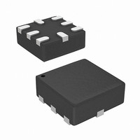
IC BUCK ADJ .5A 8-MLPQ
Manufacturer
Semtech
Type
Step-Down (Buck)r
Datasheet
1.SC195ULTRT.pdf
(20 pages)
Specifications of SC195ULTRT
Internal Switch(s)
Yes
Synchronous Rectifier
Yes
Number Of Outputs
1
Voltage - Output
0.8 ~ 3.3 V
Current - Output
500mA
Frequency - Switching
3.5MHz
Voltage - Input
2.9 ~ 5.5 V
Operating Temperature
-40°C ~ 85°C
Mounting Type
Surface Mount
Package / Case
8-MLPQ
Lead Free Status / RoHS Status
Lead free / RoHS Compliant
Power - Output
-
Other names
SC195ULTR
Available stocks
Company
Part Number
Manufacturer
Quantity
Price
Company:

Part Number:
SC195ULTRT
Manufacturer:
Semtech
Quantity:
39 722
Part Number:
SC195ULTRT
Manufacturer:
SEMTECH/美国升特
Quantity:
20 000


Applications Information
General Description
The SC195 is a synchronous step-down Pulse Width
Modulated (PWM) DC-DC regulator utilizing a 3.5MHz
fixed-frequency voltage mode architecture. The device is
designed to operate in fixed-frequency PWM mode and
enter power save (PSAVE) mode utilizing pulse frequency
modulation under light load conditions to maximize effi-
ciency. The device requires only two capacitors and a
single inductor to be implemented in most systems. The
switching frequency has been chosen to minimize the size
of the inductor and capacitors while maintaining high
efficiency. The output voltage is programmable, eliminat-
ing the need for external programming resistors. Loop
compensation is also internal, eliminating the need for
external components to control stability.
Programmable Output Voltage
The SC195 has 15 fixed output voltage levels which can be
individually selected by programming the CTL control
pins (CTL3-0 — see Table 1 on page 2 for settings). The
device is disabled whenever all four CTL pins are pulled
low and enabled whenever at least one of the CTL pins is
pulled high. This configuration eliminates the need for a
dedicated enable pin. Each CTL pin is internally pulled
down via 1MΩ if V
control pin is below the input high voltage. This ensures
that the output is disabled when power is applied if there
are no inputs to the CTL pins. Each weak pull-down is dis-
abled whenever its pin is pulled high and remains disabled
until all CTL pins are pulled low.
The output voltage can be set using different approaches.
If a static output voltage is required, the CTL pins can be
tied to either IN or GND to set the desired voltage when-
ever power is applied at IN. If enable control is required,
each CTL pin can be tied to either GND or to a micropro-
cessor I/O line to create the desired control code whenever
the control signal is forced high. This approach is equiva-
lent to using the CTL pins collectively as a single enable
pin. A third option is to connect each of the four CTL pins
to individual microprocessor I/O lines. Any of the 15
output voltages can be programmed using this approach.
If only two output voltages are needed, the CTL pins can
be combined in a way that will reduce the number of I/O
lines to 1, 2, or 3, depending on the control code for each
desired voltage. Other CTL pins could be hard wired to
IN
is below 1.5V or if the voltage on the
GND or IN. This option allows dynamic voltage adjust-
ment for systems that reduce the supply voltage when
entering sleep states. Note that applying all zeros to the
CTL pins when changing the output voltages will tempo-
rarily disable the device, so it is important to avoid this
combination when dynamically changing levels.
Adjustable Output Voltage Selection
If an output voltage other than one of the 15 program-
mable settings is needed, an external resistor divider
network can be added to the SC195 to adjust the output
voltage setting. This network scales the output based on
the resistor ratio and the programmed output setting.
The resistor values can be determined using the
equation
where V
setting selected by the CTL pins, R
between the output capacitor and the OUT pin, R
resistor between the OUT pin and ground, and I
leakage current into the OUT pin during normal opera-
tion. The current into the OUT pin is typically 1µA, so the
last term of the equation can be neglected if the current
through R
value of 10kΩ or lower will simplify the design. If I
neglected and R
the equation
Inserting resistance in the feedback loop will adversely
affect the system’s transient performance if feed-forward
capacitance is not included in the circuit. The circuit in
Figure 1 illustrates how the resistor divider and feed-
forward capacitor can be added to the SC195 schematic.
The value of feed-forward capacitance needed can be
determined using the equation
V
C
OUT
R
FF
FB
OUT
1
4
FB2
V
is the desired output voltage, V
SET
R
is much larger than 1µA. Selecting a resistor
10
FB
2
6
FB2
R
V
FB
R
is fixed, R
R
OUT
1
FB
FB
V
R
1
2
SET
V
FB
V
V
OUT
2
SET
SET
FB1
I
V
LEAK
V
OUT
can be determined using
SET
R
0
V
FB
5 .
SET
1
FB1
2
SET
is the resistor
0
is the voltage
5 .
LEAK
FB2
is the
is the
LEAK
12
is
Related parts for SC195ULTRT
Image
Part Number
Description
Manufacturer
Datasheet
Request
R


Part Number:
Description:
EVALUATION BOARD
Manufacturer:
Semtech
Datasheet:
Part Number:
Description:
EVALUATION BOARD
Manufacturer:
Semtech
Datasheet:
Part Number:
Description:
VOLTAGE SUPPRESSOR, TRANSIENT SEMTECH
Manufacturer:
Semtech
Datasheet:

Part Number:
Description:
HIGH VOLTAGE CAPACITORS MONOLITHIC CERAMIC TYPE
Manufacturer:
Semtech Corporation
Datasheet:
Part Number:
Description:
EZ1084CM5.0 AMP POSITIVE VOLTAGE REGULATOR
Manufacturer:
Semtech Corporation
Datasheet:
Part Number:
Description:
3.0 AMP LOW DROPOUT POSITIVE VOLTAGE REGULATORS
Manufacturer:
Semtech Corporation
Datasheet:
Part Number:
Description:
Manufacturer:
Semtech Corporation
Datasheet:
Part Number:
Description:
RailClamp Low Capacitance TVS Diode Array
Manufacturer:
Semtech Corporation
Datasheet:
Part Number:
Description:
Manufacturer:
Semtech Corporation
Datasheet:
Part Number:
Description:
Manufacturer:
Semtech Corporation
Datasheet:
Part Number:
Description:
Manufacturer:
Semtech Corporation
Datasheet: