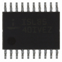
ISL8540IVEZ Intersil, ISL8540IVEZ Datasheet - Page 14

ISL8540IVEZ
Manufacturer Part Number
ISL8540IVEZ
Description
IC REG 2A DC/DC STEP-DN 20HTSSOP
Manufacturer
Intersil
Type
Step-Down (Buck)r
Datasheet
1.ISL8540IVEZ.pdf
(16 pages)
Specifications of ISL8540IVEZ
Internal Switch(s)
Yes
Synchronous Rectifier
Yes
Number Of Outputs
1
Voltage - Output
1.21 ~ 35 V
Current - Output
2A
Frequency - Switching
100kHz ~ 600kHz
Voltage - Input
9 ~ 40 V
Operating Temperature
-40°C ~ 85°C
Mounting Type
Surface Mount
Package / Case
20-TSSOP Exposed Pad, 20-eTSSOP, 20-HTSSOP
Power - Output
3W
Rohs Compliant
Yes
Lead Free Status / RoHS Status
Lead free / RoHS Compliant
Available stocks
Company
Part Number
Manufacturer
Quantity
Price
Company:
Part Number:
ISL8540IVEZ
Manufacturer:
Intersil
Quantity:
74
The modulator transfer function is the small-signal transfer
function of V
Gain and the output filter (L
break frequency at f
the modulator is simply the input voltage (V
peak-to-peak oscillator voltage ΔV
incorporates a feed forward loop that accounts for changes in
the input voltage. This maintains a constant modulator gain.
Modulator Break Frequency Equations
The compensation network consists of the transconductance
amplifier (internal to the ISL8540) and the impedance
networks Z
network is to provide a closed loop transfer function with the
highest 0dB crossing frequency (f
margin. Phase margin is the difference between the closed
loop phase at f
section relate the compensation network’s poles, zeros and
gain to the components (R
Figure 28. Use these guidelines for locating the poles and
zeros of the compensation network:
f LC
ΔV
FIGURE 28. VOLTAGE-MODE BUCK CONVERTER
OSC
=
------------------------------------------ -
2π x
OSC
IN
OUT
L O x C O
COMPARATOR
1
COMPENSATION DESIGN AND OUTPUT
VOLTAGE SELECTION
and Z
0dB
ERROR
AMP
DETAILED COMPENSATION COMPONENTS
C
V
ISL8540
/V
E/A
10
PWM
E/A
and 180°. The equations in the following
V
LC
FB
Z
+
-
OUT
FB
-
+
COMP
. This function is dominated by a DC
. The goal of the compensation
and a zero at f
C
REFERENCE
6
REFERENCE
g
=
2
O
m
, R
-
+
1.20
14
and C
DRIVER
DRIVER
R
f ESR
3
Z
4
, R
IN
×
OSC
0dB
4
⎛
⎜
⎝
O
=
1
, R
FB
), with a double pole
+
ESR
Z
------------------------------------------- -
2π x ESR x C O
) and adequate phase
. The ISL8540
FB
6
R
------ -
R
, C
LX
2
3
R
(PARASITIC)
⎞
⎟
⎠
V
. The DC Gain of
D
C
3
IN
10
IN
7
Z
R
1
) divided by the
, C
IN
2
L
R
ESR
6
O
6
C
, and C
O
V
OUT
(EQ. 11)
V
OUT
7
) in
ISL8540
Compensation Break Frequency
Equations
Assumption: R6<<R2, R6<<R3, and C10<<C6.
Figure 29 shows an asymptotic plot of the DC/DC converter’s
gain vs frequency. The actual Modulator Gain has a high gain
peak due to the high Q factor of the output filter and is not
shown in Figure 29. Using the guidelines in “Modulator Break
Frequency Equations” on page 14 should give a
Compensation Gain similar to the curve plotted. The open
loop error amplifier gain bounds the compensation gain.
Check the compensation gain at F
the error amplifier. The Closed Loop Gain is constructed on
the graph of Figure 29 by adding the Modulator Gain (in dB) to
the Compensation Gain (in dB). This is equivalent to
multiplying the modulator transfer function to the
compensation transfer function and plotting the gain.
The compensation gain uses external impedance networks
Z
loop. A stable control loop has a gain crossing with
-20dB/decade slope and a phase margin greater than 45°.
Include worst case component variations when determining
phase margin.
f
f
FIGURE 29. ASYMPTOTIC BODE PLOT OF CONVERTER GAIN
1. Pick Gain (R
2. Place 1
3. Place 2
4. Place 1
5. Place 2
6. Check Gain against Error transconductance’s Open-
7. Estimate Phase Margin - Repeat if Necessary.
Z1
Z2
FB
100
-20
-40
-60
80
60
40
20
bandwidth.
Loop Gain.
=
=
0
and Z
--------------------------------------------------------- -
2π
-------------------------- -
2πR
10
(R
20LOG
⋅
MODULATOR
4
IN
(
--------------------------------- - C
1
2
/R
ST
R
ND
ST
ND
⋅
2
4
to provide a stable, high bandwidth (BW) overall
C
GAIN
)
100
⋅
Zero Below Filter’s Double Pole (~75% f
7
Pole at the ESR Zero.
g
Zero at Filter’s Double Pole.
Pole at Half the Switching Frequency.
g
1
m
m
3
gm/(R
+
1
)
1k
F
⋅
Z1
2
F
FREQUENCY (Hz)
6
+R
LC
F
Z2
3
10k
) for desired converter
f
f
P1
P2
F
F
P1
ESR
(V
=
=
P2
IN
100k
20LOG
-------------------------- -
2πR
-----------------------------
2πR
F
/ΔV
with the capabilities of
P2
OSC
1
6
4
1
OPEN LOOP
ERROR AMP GAIN
⋅
⋅
C
C
1M
)
7
10
COMPENSATION
CLOSED LOOP
September 9, 2008
10M
GAIN
GAIN
LC
(EQ. 12)
FN6495.5
).


