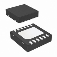
LM3668SD-2833/NOPB National Semiconductor, LM3668SD-2833/NOPB Datasheet - Page 14

LM3668SD-2833/NOPB
Manufacturer Part Number
LM3668SD-2833/NOPB
Description
IC CONV DC/DC 1A B/B HE 12-LLP
Manufacturer
National Semiconductor
Series
PowerWise®r
Type
Step-Down (Buck), Step-Up (Boost)r
Datasheet
1.LM3668SD-3034NOPB.pdf
(18 pages)
Specifications of LM3668SD-2833/NOPB
Internal Switch(s)
Yes
Synchronous Rectifier
Yes
Number Of Outputs
1
Voltage - Output
2.8 ~ 3.3 V
Current - Output
1A
Frequency - Switching
2.2MHz
Voltage - Input
2.5 ~ 5.5 V
Operating Temperature
-40°C ~ 85°C
Mounting Type
Surface Mount
Package / Case
12-LLP
Lead Free Status / RoHS Status
Lead free / RoHS Compliant
Power - Output
-
Other names
LM3668SD-2833TR
Available stocks
Company
Part Number
Manufacturer
Quantity
Price
Part Number:
LM3668SD-2833/NOPB
Manufacturer:
TI/德州仪器
Quantity:
20 000
www.national.com
In the buck PFM operation, P2 is always turned on and N2 is
always turned off , P1 and N1 power switches are switching.
P1 and N1 are turned off to enter " sleep mode" when the
output voltage reaches the "high" comparator threshold. In
boost PFM operation, P2 and N2 are switching. P1 is turned
on and N1 is turned off when the output voltage is below the
"high" threshold. Unlike in buck mode, all four power switches
are turned off to enter "sleep" mode when the output voltage
reaches the "high" threshold in boost mode. In addition, the
internal current sensing of the I
precise condition to switch over to buck or boost mode via the
PFM generator.
CURRENT LIMIT PROTECTION
The LM3668 has current limit protection to prevent excessive
stress on itself and external components during overload con-
ditions. The internal current limit comparator will disable the
power device at a typical switch peak current limit of 1.85A
(typ.).
UNDERVOLTAGE PROTECTION
The LM3668 has an UVP comparator to turn the power device
off in case the input voltage or battery voltage is too low . The
typical UVP threshold is around 2V.
SHORT CIRCUIT PROTECTION
When the output of the LM3668 is shorted to GND, the current
limit is reduced to about half of the typical current limit value
until the short is removed.
SHUTDOWN
When the EN pin is pulled low, P1 and P2 are off; N1 and N2
are turned on to pull SW1 and SW2 to ground.
THERMAL SHUTDOWN
The LM3668 has an internal thermal shutdown function to
protect the die from excessive temperatures. The thermal
shutdown trip point is typically 150°C; normal operation re-
sumes when the temperature drops below 125°C.
STARTUP
The LM3668 has a soft-start circuit that smooth the output
voltage and ramp current during startup. During startup the
bandgap reference is slowly ramped up and switch current
limit is reduced to half the typical value. Soft start is activated
only if EN goes from logic low to logic high after V
FIGURE 7. V
OUT
vs V
PFM
IN
is used to determine the
Transition
IN
reaches
14
2.5V. The startup time thereby depends on the output capac-
itor and load current demanded at startup. It is not recom-
mended to start up the device at full load while in soft-start.
Application Information
SYNC/MODE PIN
If the SYNC/MODE pin is set high, the device is set to operate
at PWM mode only. If SYNC/MODE pin is set low, the device
is set to automatically transition from PFM to PWM or PWM
to PFM depending on the load current. Do not leave this pin
floating. The SYNC/MODE pin can also be driven by an ex-
ternal clock to set the desired switching frequency between
1.6MHz to 2.7MHz.
V
The LM3668 has built in logic for conveniently setting the out-
put voltage, for example if V
with V
to use this function for dynamically switching between 2.8V
and 3.3V or switching at maximum load.
MAXIMUM CURRENT
The LM3668 is designed to operate up to 1A. For input volt-
ages at 2.5V, the maximum operating current is 600mA and
800mA for 2.7V input voltage. In any mode it is recommended
to avoid starting up the device at minimum input voltage and
maximum load. Special attention must be taken to avoid op-
erating near thermal shutdown when operating in boost mode
at maximum load (1A). A simple calculation can be used to
determine the power dissipation at the operating condition;
P
resistance θ
mum operating ambient of 85°C. As a result, the maximum
power dissipation using the above formula is around
1176mW. Refer to dissipation table below for P
different ambient temperatures.
34°C/W ( 4
layers board
per JEDEC
standard)
SEL
D-MAX
PIN
θ
SEL
JA
= (T
low the output is set to 2.8V. It is not recommended
J-MAX-OP
JA
= 34°C/W
Dissipation Rating Table
T
2941mW
A
– T
≤
25°C
A-MAX
((Note
SEL
)/θ
20191414
high, the output is set to 3.3V;
JA
T
3) and
1912mW
. The LM3668 has thermal
A
≤
60°C
(Note
6)), and maxi-
D-MAX
T
1176mW
A
≤
value at
85°C


