LM3668SD-2833/NOPB National Semiconductor, LM3668SD-2833/NOPB Datasheet
LM3668SD-2833/NOPB
Specifications of LM3668SD-2833/NOPB
Available stocks


Related parts for LM3668SD-2833/NOPB


LM3668SD-2833/NOPB Summary of contents
Page 1
... Typical Applications Typical Application Circuit © 2011 National Semiconductor Corporation LM3668 Features ■ 45µA typical quiescent current ■ ...
Page 2
Functional Block Diagram www.national.com FIGURE 1. Functional Block Diagram 2 20191404 ...
Page 3
... Die Attach Pad, connect the DAP to SGND on PCB layout to enhance thermal performance. It should not be used as a primary ground connection. Ordering Information Order Number LM3668SD - 2833 LM3668SDX - 2833 LM3668SD - 3034 LM3668SDX - 3034 LM3668SD - 4550 LM3668SDX - 4550 Note example option is 3.0V/3.4V, when V OUT options. 20191402 Description ) to set output Voltage ...
Page 4
... Absolute Maximum Ratings If Military/Aerospace specified devices are required, please contact the National Semiconductor Sales Office/ Distributors for availability and specifications Pin, SW1, SW2 & IN, DD OUT Voltage to SGND & PGND FB, EN ,MODE, SYNC pins: PGND to SGND Continuous Power Dissipation (Note ...
Page 5
Typical Performance Characteristics C = 10µ 22µF (Note 8 25°C , unless otherwise stated. IN OUT A Supply Current vs. Temperature (Not switching 3.4V) OUT NFET_RDS (on) vs. Temperature (V = 3.4V) OUT ILIMIT ...
Page 6
Efficiency at V OUT (Auto Mode) Efficiency at V OUT (Auto Mode) Efficiency at V OUT (Auto Mode) www.national.com = 2.8V 20191428 = 3.0V 20191417 = 3.3V 20191476 6 Efficiency 3.0V OUT (Forced PWM Mode) 20191473 Efficiency ...
Page 7
Efficiency 3.4V OUT (Auto Mode) 20191478 Efficiency 4.5V OUT (Auto Mode) 20191474 Efficiency 5.0V OUT (Auto Mode) 20191470 Efficiency at V OUT (Forced PWM Mode) Efficiency at V OUT (Forced PWM ...
Page 8
Line Transient in Boost Mode ( V = 3.4V, Load = 500mA) OUT Load Transient in Buck Mode (Forced PWM Mode 4.2V 3.4V, Load = 0-500mA IN OUT Load Transient in Buck-Boost Operation (Forced PWM Mode) ...
Page 9
Load Transient in Boost Mode (Forced PWM Mode 2.7V 3.0V, Load = 0-500mA IN OUT Load Transient in Buck Mode (Auto Mode 4.2V 3.3V, Load = 50-150mA IN OUT Load Transient in ...
Page 10
Load Transient in Boost Mode (Forced PWM Mode 3.5V 5.0V, Load = 0-500mA IN OUT Typical Switching Waveform in Buck Mode (PWM Mode 3.6V 3.0V, Load = 500mA IN OUT Typical Switching ...
Page 11
Typical Switching Waveform in Buck Mode (PWM Mode 4V 3.4V, Load = 500mA IN OUT Typical Switching Waveform in Buck Mode (PFM Mode 4V 3.4V, Load = 50mA IN OUT Start up ...
Page 12
Circuit Description The LM3668, a high-efficiency Buck or Boost DC-DC con- verter, delivers a constant voltage from either a single Li-Ion or three cell NIMH/NiCd battery to portable devices such as mobile phones and PDAs. Using a voltage mode architecture ...
Page 13
A. The inductor current reaches zero. B. The peak inductor current drops below the I /80 Ω ). (Typically I < 45mA + V MODE IN In PFM operation, the compensation circuit in the error am- plifier is ...
Page 14
FIGURE OUT IN In the buck PFM operation always turned on and N2 is always turned off , P1 and N1 power switches are switching. P1 and N1 are turned off to enter " ...
Page 15
INDUCTOR SELECTION There are two main considerations when choosing an induc- tor: the inductor should not saturate, and the inductor current ripple should be small enough to achieve the desired output voltage ripple. Different saturation current rating specifica- tions are ...
Page 16
Note that the output voltage ripple is dependent on the induc- tor current ripple and the equivalent series resistance of the output capacitor (R ). ESR Model 10 µF for C (For 4.5/5V option, use 10V or higher rating capacitor) ...
Page 17
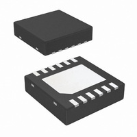
Physical Dimensions inches (millimeters) unless otherwise noted 12–Pin LLP NS Package Number SDF12A 17 www.national.com ...
Page 18
... For more National Semiconductor product information and proven design tools, visit the following Web sites at: www.national.com Products Amplifiers www.national.com/amplifiers Audio www.national.com/audio Clock and Timing www.national.com/timing Data Converters www.national.com/adc Interface www.national.com/interface LVDS www.national.com/lvds Power Management www.national.com/power Switching Regulators www.national.com/switchers LDOs www.national.com/ldo LED Lighting www ...