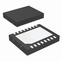
LM3370SD-3021/NOPB National Semiconductor, LM3370SD-3021/NOPB Datasheet - Page 7

LM3370SD-3021/NOPB
Manufacturer Part Number
LM3370SD-3021/NOPB
Description
IC CONV DC/DC DUAL STPDN 16-LLP
Manufacturer
National Semiconductor
Series
PowerWise®r
Type
Step-Down (Buck)r
Datasheet
1.LM3370SD-3021NOPB.pdf
(26 pages)
Specifications of LM3370SD-3021/NOPB
Internal Switch(s)
Yes
Synchronous Rectifier
Yes
Number Of Outputs
2
Voltage - Output
1.2V, 3.3V
Current - Output
600mA
Frequency - Switching
2MHz
Voltage - Input
2.7 ~ 5.5 V
Operating Temperature
-30°C ~ 85°C
Mounting Type
Surface Mount
Package / Case
16-LLP
Power - Output
1.54W
For Use With
LM3370SD-3021EV - BOARD EVALUATION LM3370SD-3021
Lead Free Status / RoHS Status
Lead free / RoHS Compliant
Other names
LM3370SD-3021TR
Note 1: Absolute Maximum Ratings are limits beyond which damage to the device may occur. Operating Ratings are conditions under which operation of the
device is guaranteed. Operating Ratings do not imply guaranteed performance limits. For guaranteed performance limits and associated test conditions, see the
Electrical Characteristics tables.
Note 2: All voltages are with respect to the potential at the GND pin.
Note 3: Internal thermal shutdown circuitry protects the device from permanent damage. The thermal shutdown engages at T
at T
Note 4: For detailed soldering specifications and information, please refer to National Semiconductor Application Note 1187: Leadless Leadframe Package (LLP)
(AN-1187).
Note 5: The Human body model is a 100 pF capacitor discharged through a 1.5 kΩ resistor into each pin. (MIL-STD-883 3015.7) The machine model is a 200
pF capacitor discharged directly into each pin. (EAIJ)
Note 6: In applications where high power dissipation and/or poor package thermal resistance is present, the maximum ambient temperature may have to be de-
rated. Maximum ambient temperature (T
of the device in the application (P
equation: T
Note 7: Junction-to-ambient thermal resistance (θ
JEDEC standard JESD51-7. The test board is a 4-layer FR-4 board measuring 102 mm x 76 mm x 1.6 mm with a 2 x 1 array of thermal vias. Thickness of copper
layers are 2/1/1/2oz.
Junction-to-ambient thermal resistance is highly application and board-layout dependent. In applications where high maximum power dissipation exists, special
care must be paid to thermal dissipation issues in board design.
The value of θ
power dissipation exists (high V
Application Note 1187: Leadless Leadframe Package (LLP) and the Power Efficiency and Power Dissipation section of this datasheet.
Note 8: Min. and Max are guaranteed by design, test and/or statistical analysis. All electrical characteristics having room-temperature limits are tested during
production with T
statistical process control.
Note 9: Guaranteed by design.
Note 10: Input voltage range for all voltage options is 2.7V to 5.5V. The voltage range recommended for the specified output voltages:
V
or
V
Note 11: Test condition: for V
Dissipation Rating Table
IN
IN,MIN
J
= 2.7V to 5.5V for 1V
= 140°C(typ.).
50°C/W (4-Layer Board) 20-bump micro SMD
= I
LOAD
A-MAX
26°C/W (4-Layer Board) LLP-16
JA
* (R
= T
of this product can vary significantly, depending on PCB material, layout, and environmental conditions. In applications where high maximum
J
= 25°C. All hot and cold limits are guaranteed by correlating the electrical characteristics to process and temperature variations and applying
DSON_PFET
J-MAX-OP
≤
V
– (θ
+ R
OUT
OUT
θ
JA
IN
DCR_INDUCTOR
D-MAX
less than 2.5V, V
JA
, high I
≤
× P
1.7V and for V
), and the junction-to-ambient thermal resistance of the part/package in the application (θ
D-MAX
A-MAX
OUT
).
), special care must be paid to thermal dissipation issues. For more information on these topics, please refer to
) is dependent on the maximum operating junction temperature (T
) + V
JA
OUT
IN
OUT
) is taken from a thermal modeling result, performed under the conditions and guidelines set forth in the
= 3.6V; for V
= 1.8V or greater, V
OUT
greater than or equal to 2.5V, V
IN
= V
7
OUT
+ 1V
Power Rating
T
1300 mW
A
= 60°C
IN
= V
OUT
J-MAX-OP
+ 1V.
= 125ºC), the maximum power dissipation
J
= 150°C (typ.) and disengages
JA
), as given by the following
Power Rating
T
1538 mW
800 mW
A
= 85°C
www.national.com


