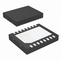
LM3370SD-3021/NOPB National Semiconductor, LM3370SD-3021/NOPB Datasheet - Page 6

LM3370SD-3021/NOPB
Manufacturer Part Number
LM3370SD-3021/NOPB
Description
IC CONV DC/DC DUAL STPDN 16-LLP
Manufacturer
National Semiconductor
Series
PowerWise®r
Type
Step-Down (Buck)r
Datasheet
1.LM3370SD-3021NOPB.pdf
(26 pages)
Specifications of LM3370SD-3021/NOPB
Internal Switch(s)
Yes
Synchronous Rectifier
Yes
Number Of Outputs
2
Voltage - Output
1.2V, 3.3V
Current - Output
600mA
Frequency - Switching
2MHz
Voltage - Input
2.7 ~ 5.5 V
Operating Temperature
-30°C ~ 85°C
Mounting Type
Surface Mount
Package / Case
16-LLP
Power - Output
1.54W
For Use With
LM3370SD-3021EV - BOARD EVALUATION LM3370SD-3021
Lead Free Status / RoHS Status
Lead free / RoHS Compliant
Other names
LM3370SD-3021TR
www.national.com
V
V
I
I
I
R
(LLP)
R
(micro SMD)
F
I
V
V
POWER ON RESET THRESHOLD/FUNCTION (POR)
nPOR1 &
nPOR2
Delay Time
POR
Threshold
Q
Q
LIM
EN
OSC
FB
OUT
IL
IH
DS_ON
DS_ON
Absolute Maximum Ratings
If Military/Aerospace specified devices are required,
please contact the National Semiconductor Sales Office/
Distributors for availability and specifications.
Electrical Characteristics
appearing in boldface type apply over the entire junction temperature range (T
V
Symbol
PFM
SD
V
SGND
PGND to SGND
SDA, SCL, EN, EN2, nPOR1,
nPOR2, SW1, SW2, FB1 & FB2 (GND - 0.2) to (V
Maximum Continuous Power
Dissipation (P
Junction Temperature (T
Storage Temperature Range
Maximum Lead Temperature
IN1
IN1
(Soldering)
= V
, V
IN2
IN2
VDD to PGND &
= 3.6V.
Feedback Voltage
Line Regulation
Load Regulation
Quiescent Current “On”
Quiescent Current “Off”
Peak Switching Current Limit
PFET
NFET
PFET
NFET
Internal Oscillator Frequency
Enable (EN) Input Current
Enable Logic Low
Enable Logic High
nPOR1 = Power ON Reset
for Buck 1
nPOR2 = Power ON Reset
for Buck 2
Percentage of Target V
D_MAX
) (Note 3)
Parameter
J-MAX
)
OUT
Internally Limited
−65°C to +150°C
-0.2V to +0.2V
(Notes 2, 8, 10)Typical limits appearing in normal type apply for T
(Note 11)
2.7V
I
100 mA
V
PFM Mode, Both Bucks ON
EN1 = EN2 = 0V
V
V
V
V
V
50 mS (default)
Can be pre-trimmd to 50 uS, 100
mS & 200 mS
V
V
pre-trimmed to 70% or 94%
O
(Notes 1, 2)
−0.2V to 6V
IN
IN
IN
IN
IN
IN
OUT
OUT
= 10 mA, V
= 3.6V, V
= 3.6V
= 3.6V, I
= 3.6V, I
= 3.6V, I
= 3.6V, I
IN
(Note 4)
≤
Falling, 85% (default), Can be
Rising
+ 0.2V)
125°C
V
≤
IN
I
≤
O
Conditions
SW
SW
SW
SW
OUT
≤
5.5V
OUT
600 mA
= 200 mA
= 200 mA
= 200 mA
= 200 mA
= 1.8V
6
= 1.8V
Operating Ratings
Thermal Properties
ESD Ratings (Note 5)
All Pins
Input Voltage Range ((Note 10))
Recommended Load Current Per
Channel
Junction Temperature (T
Ambient Temperature (T
6)
Junction-to-Ambient Thermal Resistance
θ
θ
JA
JA
(LLP-16)
(20-Bump micro SMD)
A
= T
J
= −30°C to +85°C). Unless otherwise noted,
Min
-3.5
850
1.5
1.0
A
J
) Range
) Range (Note
0.0013
0.031
1200
0.01
Typ
390
240
350
170
0.2
2.0
34
50
94
85
(Notes 1, 2)
(Note 7)
1400
Max
+3.5
500
350
400
210
−30°C to +125°C
2.4
0.4
J
0 mA to 600 mA
3
1
−30°C to +85°C
= 25°C. Limits
2.7V to 5.5V
2 kV HBM
200V MM
26°C/W
50°C/W
%/mA
Units
MHz
%/V
mA
mΩ
mΩ
mS
µA
µA
µA
%
%
V
V


