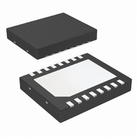
LM3370SD-3021/NOPB National Semiconductor, LM3370SD-3021/NOPB Datasheet - Page 21

LM3370SD-3021/NOPB
Manufacturer Part Number
LM3370SD-3021/NOPB
Description
IC CONV DC/DC DUAL STPDN 16-LLP
Manufacturer
National Semiconductor
Series
PowerWise®r
Type
Step-Down (Buck)r
Datasheet
1.LM3370SD-3021NOPB.pdf
(26 pages)
Specifications of LM3370SD-3021/NOPB
Internal Switch(s)
Yes
Synchronous Rectifier
Yes
Number Of Outputs
2
Voltage - Output
1.2V, 3.3V
Current - Output
600mA
Frequency - Switching
2MHz
Voltage - Input
2.7 ~ 5.5 V
Operating Temperature
-30°C ~ 85°C
Mounting Type
Surface Mount
Package / Case
16-LLP
Power - Output
1.54W
For Use With
LM3370SD-3021EV - BOARD EVALUATION LM3370SD-3021
Lead Free Status / RoHS Status
Lead free / RoHS Compliant
Other names
LM3370SD-3021TR
Application Information
SETTING OUTPUT VOLTAGE VIA I
The outputs of the LM3370 can be programmed through Buck
1 & Buck 2 registers via I
dynamically adjusted between 1V to 2V in 50 mV steps and
Buck 2 output voltage can be adjusted between 1.8V to 3.3V
in 100 mV steps. Finer adjustments to the output of Buck 2
can be achieved with the placement of a resistor betweeen
VOUT2 and the FB2 pin. Typically by placing a 20KΩ resistor,
R, between these nodes will result in the programmed Output
Voltage increasing by approximately 45mV,ΔV
Please refer to for programming the desire output voltage. If
the I
age will be the pre-trimmed voltage. For example,
LM3370SD-3021 refers to 1.2V for Buck 1 and 3.3V for Buck
2.
V
V
pin is not tied to V
must be set equal or greater of the two inputs ( V
An optional capacitor can be used for better noise immunity
at V
ally, for reasons of noise suppression, it is advisable to tie the
EN1/EN2 pins to V
SDA, SCL Pins
When not using I
directly to the V
Micro-Stepping:
The Micro-Stepping feature minimizes output voltage over-
shoot/undershoot during large output transients. If Micro-
stepping is enabled through I
ically ramps at 50 mV per step for Buck 1 and 100 mV per
step for Buck 2. The steps are summarized as follow:
Buck 1: 50 mV/step and 32 µs/step
Buck 2: 100 mV/step and 32 µs/step
For example if changing Buck 1 voltage from 1V to 1.8V yields
20 steps [(1.8 - 1)/ 0.05 = 20]. This translates to 640μs [(20 x
32 µs) = 640 µs] needed to reach the final target voltage.
INDUCTOR SELECTION
There are two main considerations when choosing an induc-
tor; the inductor should not saturate, and the inductor current
ripple is small enough to achieve the desired output voltage
ripple.
There are two methods to choose the inductor current rating.
method 1:
The total current is the sum of the load and the inductor ripple
current. This can be written as
•
•
•
•
DD
DD
I
V
L inductor
f switching frequency
LOAD
DD
2
Pin
is the power supply to the internal control circuit, if V
IN
C compatible feature is not used, the default output volt-
pin or when V
input voltage
load current
DD
ΔV
2
IN
C the SDA and SCL pins should be tied
pin.
DD
TYP
DD
during normal operating condition, V
rather than V
= R × 500mV / 234KΩ
is not tied to either V
2
C. Buck 1 output voltage can be
2
C, the output voltage automat-
IN
2
.
C Compatible
IN
pins. Addition-
TYP
IN1
.
or V
IN2
DD
DD
).
21
method 2:
A more conservative approach is to choose an inductor that
can handle the maximum current limit of 1400 mA.
Given a peak-to-peak current ripple (I
to be at least
A 2.2 µH inductor with a saturation current rating of at least
1400 mA is recommended for most applications. The
inductor’s resistance should be less than around 0.2Ω for
good efficiency. Table 2 lists suggested inductors and sup-
pliers.
For low-cost applications, an unshielded bobbin inductor is
suggested. For noise critical applications, a toroidal or shield-
ed-bobbin inductor should be used. A good practice is to lay
out the board with overlapping footprints of both types for de-
sign flexibility. This allows substitution of a low-noise toroidal
inductor, in the event that noise from low-cost bobbin models
is unacceptable.
Below are some suggested inductor manufacturers include
but are not limited to:
INPUT CAPACITOR SELECTION
A ceramic input capacitor of 4.7 μF, 6.3V is sufficient for most
applications. A larger value may be used for improved input
voltage filtering. The input filter capacitor supplies current to
the PFET switch of the LM3370 in the first half of each cycle
and reduces voltage ripple imposed on the input power
source. A ceramic capacitor's low ESR provides the best
noise filtering of the input voltage spikes due to this rapidly
changing current. Select an input filter capacitor with a surge
current rating sufficient for the power-up surge from the input
power source. The power-up surge current is approximately
the capacitor’s value (µF) times the voltage rise rate (V/µs).
The input current ripple can be calculated as:
OUTPUT CAPACITOR SELECTION
DC bias characteristics of ceramic capacitors must be con-
sidered when selecting case sizes like 0805 and 0603. DC
NR3010T2R2M Taiyo Yuden
NR3015T2R2M
LPO3310-222
DO3314-222
SD3114-2R2
VLF3010AT-
2R2M1R0
TABLE 2. Suggested Inductors and Suppliers
Model
Coilcraft
Vendor
Cooper
TDK
3.3 x 3.3 x 1.4
3.3 x 3.3 x 1.0
3.1 x 3.1 x 1.4
3.0 x 3.0 x 1.0
3.0 x 3.0 x 1.5
2.6 x 2.8 x 1.0
Dimensions
PP
(mm)
) the inductor needs
www.national.com
1.48A
1.48A
1.6A
1.1A
1.1A
1.0A
I
SAT


