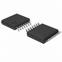
BD9845FV-E2 Rohm Semiconductor, BD9845FV-E2 Datasheet - Page 7

BD9845FV-E2
Manufacturer Part Number
BD9845FV-E2
Description
IC REG SW STEP DOWN 1CH 14-SSOP
Manufacturer
Rohm Semiconductor
Type
Step-Down (Buck)r
Datasheet
1.BD9845FV-E2.pdf
(16 pages)
Specifications of BD9845FV-E2
Internal Switch(s)
No
Synchronous Rectifier
No
Number Of Outputs
1
Current - Output
1A
Frequency - Switching
100kHz ~ 1.5MHz
Voltage - Input
3.6 ~ 35 V
Operating Temperature
-40°C ~ 85°C
Mounting Type
Surface Mount
Package / Case
14-SSOP
Power - Output
500mW
Lead Free Status / RoHS Status
Lead free / RoHS Compliant
Voltage - Output
-
Lead Free Status / Rohs Status
Lead free / RoHS Compliant
Other names
BD9845FV-E2TR
●Operation description of each block and function
© 2009 ROHM Co., Ltd. All rights reserved.
BD9845FV
www.rohm.com
1) REG (reference voltage unit)
2) ERR Amp (error amplifier)
3) OSC (triangular wave oscillating unit)
As for REG (2.5V), reference voltage (2.5V) stabilized better than supply voltage input to VCC terminal is supplied as an
operation voltage of IC internal circuit, as well as output outside through VREF terminal. Insert a capacitor of 1uF to VREF
terminal.
As for REG (VCC-5V), voltage of VCC-5V is supplied as power supply (LDO) of driver circuit (DRV) of OUT terminal, as
well as output outside through C5V terminal. Insert a capacitor of 1uF to VCC terminal of C5V terminal.
In step-down application, inverting input INV of
error amplifier detects output voltage by sending
back feedback current from final output stage (on
load side) of switching regulator. R1 and R2
connected to this input terminal are resistor for
setting output voltage. Non-inverting input of
amplifier is a reference input of error amplifier
itself by adding reference voltage (1.0V) inside IC.
Rf and Cf connected between FB, which is output
from error amplifier, and INV are for feedback of
error amplifier, and allows setting of loop gain.
FB is connected to PWM Comp and supplied as
non-inverting input.
Setting of output voltage (Vo) is as follows:
Generates triangular wave for inputting to PWM Comp.
First, timing capacitor C
inside IC. When CT voltage reaches 2.0 V typ, the comparator is switched, and then C
(200 µA). Then, when CT voltage reaches 1.5V, the comparator is switched again, and C
repetition generates triangular wave.
Oscillation frequency is determined by externally mounted C
ICT : CT sink/source current 200 uA typ
ΔVosc : Triangular wave amplifying voltage=(Vt0-Vt100)=0.50 V typ.
Here, error from theoretical formula is caused by delay of
internal circuit at a high frequency. See the graph in Fig 31 for
setting.
This triangular wave can be taken out through CT terminal. It is
also possible to input the oscillator externally by switching to
slave mode described later. Waveform input here in principle
must be triangular wave of Vpeak = (1.5V 2.0V) equivalent to
internal oscillation circuit.
External input voltage range
Standard external C
Fosc ≒ ICT/(2・C
V
C
CT :
CT :
Vo
1.4 V < V
MIN.47 pF – MAX.3000 pF
=
CT
range
CT <
R1+R2
CT
R2
CT
connected between CT terminal and GND is charged by constant current (200 uA) generated
2.3 V
・ΔVosc)
1.0V
7/15
CT
through theoretical formula below:
R1
R 2
Vo
10000
1000
100
10
10
Rf
Cf
CT
11
12
CT timing capacity (pF)
is discharged by constant current
CT
Fig.30
INV
FB
100
1V
is charged again. This
Ta=25℃
Fig.31
2009.05 - Rev.A
Technical Note
ErrAmp
1000
10000


