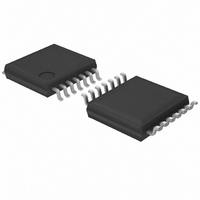
BD9845FV-E2 Rohm Semiconductor, BD9845FV-E2 Datasheet

BD9845FV-E2
Specifications of BD9845FV-E2
Related parts for BD9845FV-E2
BD9845FV-E2 Summary of contents
Page 1
... High-frequency Step-down Switching Regulator(Controller type) BD9845FV ●Overview BD9845FV containing a circuit of switching regulator controller by pulse width modulation system. This circuit can be used for step-down DC/DC converter operation. In addition, the package is designed compact, and is optimum for compact power supply for many kinds of equipment. ●Feature 1) High voltage resistance input (Vcc=35V) 2) FET driver circuit is contained (step-down circuit 1 output) ...
Page 2
... BD9845FV ●Electric characteristics (Ta=25C, VCC=6V unless otherwise specified) Item [VREF output unit] Output voltage Input stability Load stability Current capacity [Triangular wave oscillator] Oscillation frequency Frequency fluctuation [Soft start unit] SS source current SS sink current [Pause period adjusting circuit] DT input bias current ...
Page 3
... BD9845FV ●Reference data VCC= -50 - 100 125 Ambient Temperature: Ta(°C) Fig.1 Standby current temperature characteristics 2.520 2.515 2.510 2.505 Ta=25°C 2.500 2.495 2.490 2.485 2.480 Supply Voltage: VCC(V) Fig.4 VREF supply voltage characteristics 3.5 3.4 3.3 3.2 3.1 3 2.9 2.8 2.7 2 ...
Page 4
... BD9845FV ●Reference data 4.0 3.5 3.0 VCC=6.0V 2.5 2.0 1.5 1.0 0.5 0.0 0 0.2 0.4 0.6 0.8 1 1.2 1.4 1.6 SS Voltage: VSS(V) Fig.13 SS source current 120 CCP=1800pF 110 100 VCC= -50 - 100 125 Ambient Temperature: Ta(°C) Fig.16 Oscillation frequency temperature characteristics 100 ...
Page 5
... BD9845FV ●Reference data 5.0 4.5 4.0 VCC=5.0V 3.5 Ta=25°C 3.0 2.5 2.0 1.5 1.0 0.5 0 100 150 200 250 IC5V(mA) Fig.25 C5V saturation voltage www.rohm.com © 2009 ROHM Co., Ltd. All rights reserved. 5.5 5.4 VCC=6.0V 5.3 Ta=25°C 5.2 5.1 5 ...
Page 6
... BD9845FV ●Block diagram/Pin layout VCC VREF REG VREF (2.5V VREF 1V±10mV 2μ ERR - SSOFF INV OSC 200μ 2.0V - 1.5V 200μA MASTER /SLAVE CT VREF CT GND STB C5V OUT VCC Fig.29 Pin layout www.rohm.com © 2009 ROHM Co., Ltd. All rights reserved. ...
Page 7
... BD9845FV ●Operation description of each block and function 1) REG (reference voltage unit) As for REG (2.5V), reference voltage (2.5V) stabilized better than supply voltage input to VCC terminal is supplied as an operation voltage of IC internal circuit, as well as output outside through VREF terminal. Insert a capacitor of 1uF to VREF terminal ...
Page 8
... BD9845FV 4) Soft start (soft start function possible to provide SS terminal (13pin) with soft start function by as shown on the right. connecting C SS Soft start time TSS is shown by the formula below: Css : SS terminal connection capacity Tss = Css・ Vinv Vinv : Error amplifier reference voltage ...
Page 9
... BD9845FV 7) STB /SEL(Standby/Master/Slave function) Standby mode and normal mode can be switched by STB terminal (4pin). 1. When STB<0.5V, standby mode is set. Out put stop (OUT=H) and REG also stops. Circuit current is also Isc = 0 uA here. 2. When STB>3.0V, normal operation mode is set. All circuits operate. Use the controller normally in this range. ...
Page 10
... BD9845FV ●Timing chart ◎Starting characteristics (UVLO cancel) and standby operation VCC (1) UVLO (Vcc) is canceled when Vcc>3.2V. ①Vcc>3.2VでUVLO(Vcc)解除 STB VREF起動電圧 1.8Vtyp. VREF停止電圧 0.9Vtyp. VREF (2) UVLO (VREF) is canceled when VREF>2.2V. ②VREF>2.2VでUVLO(VREF)解除 ...
Page 11
... BD9845FV ●Example of application circuit VREF VREF CT INV VREF - Setting of output unit coil (L) and capacitor (Co) Set the coil and capacitor as follows in step-down application: <Setting of L-value> When load current gets heavy, the current flowing through the coil gets continuous, and the relation below is established: Tsw ...
Page 12
... BD9845FV 2) Example of overcurrent protection circuit Insert a sense resistor between the source and VIN of output Pch-FET for detecting overcurrent as shown in the figure. Refer to the formula below for determining a sense resistor and select permissible loss ensuring a margin. Vocpth Rsense = Iocp Vocpth : Overcurrent detection voltage (50 mV typ) ...
Page 13
... BD9845FV 5) About board layout In order to make full use of IC performance, fully investigate the items below in addition to general precautions. ・ Each output of OCP+/OCP- is such a sensitive circuit. When wiring is routed around easily subjected to noise. Try to make the wiring as short as possible. ・ Switching of large current is likely to generate noise. Try to make the large current route (VIN, Rsense, FET, L, Di, and Cout) as thick and short as possible, and try to apply one-point grounding for GND ...
Page 14
... BD9845FV ●Notes for use 1) About maximum absolute rating When the maximum absolute rating of application voltage or operation voltage range is exceeded, it may lead to deterioration or rupture impossible to forecast rupture in short mode or open mode. When a special mode is expected exceeding the maximum absolute rating, try to take a physical safety measure such as a fuse. ...
Page 15
... BD9845FV ●Ordering part number Part No. Part No. 9845 SSOP-B14 5.0 ± 0 0.15 ± 0.1 0.1 0.65 0.22 ± 0.1 www.rohm.com © 2009 ROHM Co., Ltd. All rights reserved Package FV : SSOP-B14 <Tape and Reel information> Tape Embossed carrier tape Quantity 2500pcs E2 Direction The direction is the 1pin of product is at the upper left when you hold ...
Page 16
No copying or reproduction of this document, in part or in whole, is permitted without the consent of ROHM Co.,Ltd. The content specified herein is subject to change for improvement without notice. The content specified herein is for the purpose ...


