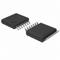
BD9845FV-E2 Rohm Semiconductor, BD9845FV-E2 Datasheet - Page 13

BD9845FV-E2
Manufacturer Part Number
BD9845FV-E2
Description
IC REG SW STEP DOWN 1CH 14-SSOP
Manufacturer
Rohm Semiconductor
Type
Step-Down (Buck)r
Datasheet
1.BD9845FV-E2.pdf
(16 pages)
Specifications of BD9845FV-E2
Internal Switch(s)
No
Synchronous Rectifier
No
Number Of Outputs
1
Current - Output
1A
Frequency - Switching
100kHz ~ 1.5MHz
Voltage - Input
3.6 ~ 35 V
Operating Temperature
-40°C ~ 85°C
Mounting Type
Surface Mount
Package / Case
14-SSOP
Power - Output
500mW
Lead Free Status / RoHS Status
Lead free / RoHS Compliant
Voltage - Output
-
Lead Free Status / Rohs Status
Lead free / RoHS Compliant
Other names
BD9845FV-E2TR
●I/O equivalent circuit diagram
© 2009 ROHM Co., Ltd. All rights reserved.
BD9845FV
www.rohm.com
5) About board layout
6) PIN processing of channel unused
CT
When only one channel is used, process unused channels as shown above.
In order to make full use of IC performance, fully investigate the items below in addition to general precautions.
STB
・ Each output of OCP+/OCP- is such a sensitive circuit. When wiring is routed around, it is easily subjected to noise.
・ Switching of large current is likely to generate noise. Try to make the large current route (VIN, Rsense, FET, L, Di,
・ C
・ Also be careful not to allow common impedance to sense family GND.
VREF
VCC
Try to make the wiring as short as possible.
and Cout) as thick and short as possible, and try to apply one-point grounding for GND. OUT terminal is also a
switching line, and it must be wired along a distance as short as possible. (When multi-layer board is used, shielding
by intermediate layer also seems to be effective.)
protected against external influence.
4pin (STB)
CT
VREF
VCC
INV
and C
12pin (INV)
VCC
5pin (C5V)
VREF
VREF
VREF DT
2pin(CT)
VREF
1
VREF
VREF
14
VCC
VREF
are reference of all, and must be wired along the shortest distance to GND of IC stabilized to be
SS INV
13
VREF
VREF
12
VCC
Fig.43
FB
11
C5V
SEL
OCP- OCP+ VCC OUT
10pin (SEL)
9
VCC
VCC VCC
8
DT
7
6
VREF
13/15
6pin (OUT)
14pin (DT)
11pin (FB)
VREF
VCC
C5V
VCC
C5V
VREF
VREF
OUT
1pin (VREF)
FB
VCC
VCC
VREF
SS
VREF
OCP-
OCP+
3pin (GND) , 7pin (VCC)
8pin (OCP+)
9pin (OCP-)
13pin (SS)
VCC
C5V
2009.05 - Rev.A
Technical Note
VCC
C5V
GND
VREF
VCC
VREF
VCC
C5V
VCC
C5V
VCC


