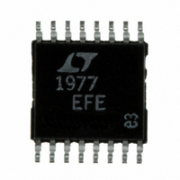
LT1977EFE#PBF Linear Technology, LT1977EFE#PBF Datasheet - Page 16

LT1977EFE#PBF
Manufacturer Part Number
LT1977EFE#PBF
Description
IC REG SW 1.5A HV STP DN 16TSSOP
Manufacturer
Linear Technology
Type
Step-Down (Buck)r
Datasheet
1.LT1977EFEPBF.pdf
(24 pages)
Specifications of LT1977EFE#PBF
Internal Switch(s)
Yes
Synchronous Rectifier
No
Number Of Outputs
1
Voltage - Output
1.2 ~ 54 V
Current - Output
1.5A
Frequency - Switching
500kHz
Voltage - Input
3.3 ~ 60 V
Operating Temperature
-40°C ~ 125°C
Mounting Type
Surface Mount
Package / Case
16-TSSOP Exposed Pad, 16-eTSSOP, 16-HTSSOP
Primary Input Voltage
60V
No. Of Outputs
1
Output Voltage
54V
Output Current
3.5A
No. Of Pins
16
Operating Temperature Range
-40°C To +125°C
Msl
MSL 1 - Unlimited
Rohs Compliant
Yes
Dc To Dc Converter Type
Step Down
Pin Count
16
Input Voltage
60V
Switching Freq
575KHz
Package Type
TSSOP EP
Output Type
Adjustable
Switching Regulator
Yes
Mounting
Surface Mount
Input Voltage (min)
2.4V
Operating Temp Range
-40C to 125C
Operating Temperature Classification
Automotive
Lead Free Status / RoHS Status
Lead free / RoHS Compliant
Power - Output
-
Lead Free Status / Rohs Status
Compliant
Available stocks
Company
Part Number
Manufacturer
Quantity
Price
LT1977
APPLICATIO S I FOR ATIO
Example: For V
During the sleep portion of the Burst Mode cycle, the V
pin voltage is held just below the level needed for normal
operation to improve transient response. See the Typical
Performance Characteristics section for burst and tran-
sient response waveforms.
If a no load condition can be anticipated, the supply current
can be further reduced by cycling the SHDN pin at a rate
higher than the natural no load burst frequency. Figure 6
shows Burst Mode operation with the SHDN pin. V
burst ripple is maintained while the average supply current
drops to 15µA. The PG pin will be active low during the
“on” portion of the SHDN waveform due to the C
tor discharge when SHDN is taken low. See the Power
Good section for further information.
CATCH DIODE
The catch diode carries load current during the SW off
time. The average diode current is therefore dependent on
the switch duty cycle. At high input to output voltage ratios
the diode conducts most of the time. As the ratio ap-
proaches unity the diode conducts only a small fraction of
the time. The most stressful condition for the diode is
when the output is short circuited. Under this condition the
diode must safely handle I
I
16
IN AVG
(
)
=
=
45
45
150
125
100
75
50
25
0
µ + µ +
µ + µ +
0
A
A
OUT
5
5
10
= 3.3V, V
U
A
A
Figure 5. I
INPUT VOLTAGE (V)
20
⎛
⎜
⎝
44
3 3
12
U
.
µ =
PEAK
30
A
⎞
⎟
⎠
IN
Q
(
125
= 12V
vs V
99
at maximum duty cycle.
40
µ
µ +
V
IN
W
OUT
A
A
T
A
50
= 25°C
= 3.3V
1977 F05
12 5
( )
0 8
.
60
.
µ +
A
U
T
0 5
capaci-
.
µ
OUT
A
)
C
Table 5. Catch Diode Selection Criteria
DIODE
IR 10BQ100
Diodes Inc.
B260SMA
Diodes Inc.
B360SMB
IR
MBRS360TR
IR 30BQ100
To maximize high and low load current efficiency a fast
switching diode with low forward drop and low reverse
leakage should be used. Low reverse leakage is critical to
maximize low current efficiency since its value over tem-
perature can potentially exceed the magnitude of the
LT1977 supply current. Low forward drop is critical for
high current efficiency since the loss is proportional to
forward drop.
These requirements result in the use of a Schottky type
diode. DC switching losses are minimized due to its low
forward voltage drop and AC behavior is benign due to its
lack of a significant reverse recovery time. Schottky diodes
are generally available with reverse voltage ratings of 60V
and even 100V and are price competitive with other types.
The effect of reverse leakage and forward drop on effi-
ciency for various Schottky diodes is shown in Table 5. As
can be seen these are conflicting parameters and the user
500mA/DIV
50mV/DIV
2V/DIV
V
V
SHDN
I
OUT
SW
Figure 6. Burst Mode with Shutdown Pin
V
V
I
Q
IN
OUT
0.0µA
0.1µA
0.2µA
0.5µA
= 15µA
25°C
1µA
= 12V
V
= 3.3V
LEAKAGE
OUT
= 3.3V
1.81mA
242µA
440µA
225µA
125°C
59µA
TIME (50ms/DIV)
V
F
0.72V
0.48V
0.45V
0.42V
0.59V
25°C
AT 1A
I
V
Q
V
OUT
I
at 125°C EFFICIENCY
IN
125µA
215µA
270µA
821µA
206µA
L
= 0A
=12V
= 3.3 V
1977 G16
OUT
V
I
76.1%
80.4%
80.8%
81.4%
78.8%
IN
L
= 1A
=12V
= 3.3V
1977fa


