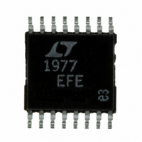
LT1977EFE#PBF Linear Technology, LT1977EFE#PBF Datasheet - Page 15

LT1977EFE#PBF
Manufacturer Part Number
LT1977EFE#PBF
Description
IC REG SW 1.5A HV STP DN 16TSSOP
Manufacturer
Linear Technology
Type
Step-Down (Buck)r
Datasheet
1.LT1977EFEPBF.pdf
(24 pages)
Specifications of LT1977EFE#PBF
Internal Switch(s)
Yes
Synchronous Rectifier
No
Number Of Outputs
1
Voltage - Output
1.2 ~ 54 V
Current - Output
1.5A
Frequency - Switching
500kHz
Voltage - Input
3.3 ~ 60 V
Operating Temperature
-40°C ~ 125°C
Mounting Type
Surface Mount
Package / Case
16-TSSOP Exposed Pad, 16-eTSSOP, 16-HTSSOP
Primary Input Voltage
60V
No. Of Outputs
1
Output Voltage
54V
Output Current
3.5A
No. Of Pins
16
Operating Temperature Range
-40°C To +125°C
Msl
MSL 1 - Unlimited
Rohs Compliant
Yes
Dc To Dc Converter Type
Step Down
Pin Count
16
Input Voltage
60V
Switching Freq
575KHz
Package Type
TSSOP EP
Output Type
Adjustable
Switching Regulator
Yes
Mounting
Surface Mount
Input Voltage (min)
2.4V
Operating Temp Range
-40C to 125C
Operating Temperature Classification
Automotive
Lead Free Status / RoHS Status
Lead free / RoHS Compliant
Power - Output
-
Lead Free Status / Rohs Status
Compliant
Available stocks
Company
Part Number
Manufacturer
Quantity
Price
APPLICATIO S I FOR ATIO
low value such that the current doesn’t continue to ratchet
higher. When the FB pin voltage is abnormally low thereby
indicating some sort of short-circuit condition, the oscil-
lator frequency will be reduced. Oscillator frequency is
reduced by a factor of 4 when the FB pin voltage is below
0.4V and increases linearly to its typical value of 500kHz at
a FB voltage of 0.95V (see Typical Performance Character-
istics). In addition, if the current in the switch exceeds 1.5
• I
the next on cycle effectively reducing the oscillator fre-
quency by a factor of 2. These oscillator frequency reduc-
tions during short-circuit conditions allow the LT1977 to
maintain current control.
SOFT-START
For applications where [V
large input surge currents can’t be tolerated, the LT1977
soft-start feature should be used to control the output
capacitor charge rate during start-up, or during recovery
from an output short circuit thereby adding additional
control over peak inductor current. The soft-start function
limits the switch current via the V
constant voltage ramp rate (dV/dt) at the output capacitor.
A capacitor (C1 in Figure 2) from the C
regulated output voltage determines the output voltage
ramp rate. When the current through the C
exceeds the C
output capacitor is limited by reducing the V
The C
Typical Performance Characteristics) and is defeated for
FB voltages greater than 0.9V (typical). The output dV/dt
can be approximated by:
but actual values will vary due to start-up load conditions,
compensation values and output capacitor selection.
Burst Mode OPERATION
To enhance efficiency at light loads, the LT1977 automati-
cally switches to Burst Mode operation (see Typical
Performance Characteristics) which keeps the output
PK
dV
dt
current demanded by the V
SS
=
threshold is proportional to the FB voltage (see
I
C
CSS
SS
SS
threshold (I
U
U
IN
/(V
CSS
OUT
C
), the voltage ramp of the
pin, the LT1977 will skip
W
+ V
C
pin to maintain a
F
)] ratios > 10 or
SS
C
SS
pin voltage.
pin to the
U
capacitor
capacitor charged to the proper voltage while minimizing
the input quiescent current. During Burst Mode opera-
tion, the LT1977 delivers short bursts of current to the
output capacitor followed by sleep periods where the
output power is delivered to the load by the output
capacitor. In addition, V
are reduced to typically 45µA and 110µA respectively
during the sleep time. As the load current decreases
towards a no load condition, the percentage of time that
the LT1977 operates in sleep mode increases and the
average input current is greatly reduced resulting in
higher efficiency.
The minimum average input current depends on the V
V
network and Schottky diode leakage. It can be approxi-
mated by the following equation:
where:
OUT
I
V
V
I
I
I
η = low current efficiency (non Burst Mode operation)
I
IN AVG
VINS
BIASS
FB
S
OUT
IN
(
= catch diode reverse leakage at V
1V/DIV
ratio, V
= feedback network current
V
= input voltage
OUT
= input pin current in sleep mode
= output voltage
= BIAS pin current in sleep mode
)
V
V
≅
IN
OUT
C
C
CSS
= 12V
I
VINS
= 3.3V
frequency compensation, feedback divider
C
= 1000pF
CSS
+
= 0.01µF
Figure 4. V
I
SHDN
IN
1ms/DIV
+
and BIAS quiescent currents
⎛
⎜
⎝
OUT
V
C
V
OUT
CSS
IN
dV/dt
= 0.1µF
⎞
⎟
⎠
(
I
BIASS
OUT
1977 F04
LT1977
( )
+
η
I
FB
15
+
I
S
IN
1977fa
)
to


