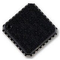
ADP3209DJCPZ-RL ON Semiconductor, ADP3209DJCPZ-RL Datasheet

ADP3209DJCPZ-RL
Specifications of ADP3209DJCPZ-RL
Available stocks
Related parts for ADP3209DJCPZ-RL
ADP3209DJCPZ-RL Summary of contents
Page 1
ADP3209D 5-Bit, Programmable, Single-Phase, Synchronous Buck Controller The ADP3209D is a highly efficient, single−phase, synchronous buck switching regulator controller. With its integrated drivers, the ADP3209D is optimized for converting the notebook battery voltage to render the supply voltage required by ...
Page 2
COMP FB REF LLINE PWRGD FBRTN ABSOLUTE MAXIMUM RATINGS Parameter VCC FBRTN, PGND BST DC t < 200 ns BST < 200 ns DRVH DRVL to PGND DC t < 200 ns ...
Page 3
PIN FUNCTION DESCRIPTIONS Pin No Mnemonic 1 FBRTN Feedback Return Input/Output. This pin remotely senses the GMCH voltage also used as the ground return for the VID DAC and the voltage error amplifier blocks Voltage Error ...
Page 4
ELECTRICAL CHARACTERISTICS V otherwise noted (Note 1). Current entering a pin (sunk by the device) has a positive sign. R Parameter Symbol VOLTAGE CONTROL − Voltage Error Amplifier (VEAMP) FB, LLINE Voltage LLINE Range (Note 2) ...
Page 5
ELECTRICAL CHARACTERISTICS V otherwise noted (Note 1). Current entering a pin (sunk by the device) has a positive sign. R Parameter Symbol VOLTAGE MONITORING AND PROTECTION − Power Good PWRGD Latchoff Delay T LOFFPWRGD PWRGD Propagation T PDPWRGD Delay (Note ...
Page 6
ELECTRICAL CHARACTERISTICS V otherwise noted (Note 1). Current entering a pin (sunk by the device) has a positive sign. R Parameter Symbol RAMP GENERATOR RAMP Voltage V RAMP RAMP Current Range I RAMP (Note 2) PWM COMPARATOR PWM Comparator V ...
Page 7
ELECTRICAL CHARACTERISTICS otherwise noted (Note 1). Current entering a pin (sunk by the device) has a positive sign. R Parameter Symbol HIGH−SIDE MOSFET DRIVER Pullup Resistance, Sourcing Current Pulldown Resistance, Sinking Current Transition Times tr DRVH tf DRVH Dead Delay ...
Page 8
TYPICAL PERFORMANCE CHARACTERISTICS VID 450 400 350 SWITCHING FREQUENCY 300 250 OUTPUT RIPPLE 200 150 INPUT = 12 V LOAD = 10 A 100 0.25 0.5 0.75 1 OUTPUT VOLTAGE (V) Figure 3. Switching Frequency ...
Page 9
TYPICAL PERFORMANCE CHARACTERISTICS VID OUTPUT VOLTAGE Figure 9. Load Transient OUTPUT VOLTAGE SWITCH NODE Figure 11. Load Transient 20°C to 100°C, unless ...
Page 10
Theory of Operation The ADP3209D is a ramp−pulse−modulated (RPM) controller for synchronous buck Intel GMCH core power supply. The internal 5−bit VID DAC conforms to the Intel IMVP−6+ specifications. The ADP3209D is a stable, high performance architecture that includes • ...
Page 11
RAMP CLOCK OSCILLATOR 0.2 V VCC RAMP COMP Setting Switch Frequency Master Clock Frequency in PWM Mode When the ADP3209D runs in PWM, the clock ...
Page 12
Output inductor ESR sensing without the use of a thermistor for the lowest cost • Output inductor ESR sensing with ...
Page 13
The ADP3209D provides a soft transient function to reduce inrush current during VID transitions. Reducing the inrush current helps decrease the acoustic noise generated by the MLCC input capacitors and inductors. The soft transient feature is implemented internally. When a ...
Page 14
OFF L ON Figure 19. Buck Topology Inductor Current During t and OFF L OFF Figure 20. Buck Topology Inductor Current During t and INDUCTOR CURRENT SWITCH NODE VOLTAGE ...
Page 15
CSREF PWRGD 2 DRVH 4 DRVL 1 CH1 5.00V CH2 5.00V M2.00ms CH3 1.00V CH4 20.0V Figure 23. ADP3209D RVP Function Output Enable and UVLO For the ADP3209D to begin switching, the VCC supply voltage to the controller must ...
Page 16
VID4 VID3 VID2 VID1 VID0 ...
Page 17
Application Information The design parameters for a typical IMVP−6+ compliant GPU core VR application are as follows: • Maximum input voltage ( INMAX • Minimum input voltage ( 8.0 V INMIN • Output voltage ...
Page 18
Because R = 280 kW, the following resistance sets up R 300 kHz switching frequency in RPM operation. 2 280 0.061 ) 0 RPM 1.150 V ) 1.0 V 462 Inductor ...
Page 19
Inductor DCR Temperature Correction If the DCR of the inductor is used as a sense element and copper wire is the source of the DCR, the temperature changes associated with the inductor’s winding must be compensated for. Fortunately, copper has ...
Page 20
x(MIN) V OSMAX VID X(MAX VID VID where: ...
Page 21
MOSFET S(MF where the total number of main MOSFETs the total gate ...
Page 22
R is the current limit resistor. R LIM LIM ILIM pin to ground the output load line resistance the current limit set point. This is the peak inductor LIM current that will trip current ...
Page 23
...
Page 24
Measure the output ripple with no load and with a full load with scope, making sure both are within the specifications. Set the AC Load Line 1. Remove the dc load from the circuit and connect a dynamic load. ...
Page 25
V TRANREL Figure 30. Transient Setting Waveform, Load Release Layout and Component Placement The following guidelines are recommended for optimal performance of a switching regulator system. General Recommendations 1. For best results, use a PCB of four ...
Page 26
... The CSREF signal should be Kelvin connected to ORDERING INFORMATION Device Temperature Range ADP3209DJCPZ−RL 0°C to 100°C †For information on tape and reel specifications, including part orientation and tape sizes, please refer to our Tape and Reel Packaging Specifications Brochure, BRD8011/D. *The “Z” suffix indicates Pb−Free part. ...
Page 27
... C NOTE 3 PACKAGE OUTLINE *For additional information on our Pb−Free strategy and soldering details, please download the ON Semiconductor Soldering and Mounting Techniques Reference Manual, SOLDERRM/D. N. American Technical Support: 800−282−9855 Toll Free USA/Canada Europe, Middle East and Africa Technical Support: Phone: 421 33 790 2910 Japan Customer Focus Center Phone: 81− ...


