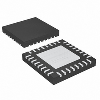
MAX17003ETJ+ Maxim Integrated Products, MAX17003ETJ+ Datasheet - Page 33

MAX17003ETJ+
Manufacturer Part Number
MAX17003ETJ+
Description
IC PS CTRLR FOR NOTEBOOKS 32TQFN
Manufacturer
Maxim Integrated Products
Datasheet
1.MAX17003ETJ.pdf
(36 pages)
Specifications of MAX17003ETJ+
Applications
Controller, Notebook Computers
Voltage - Input
6 ~ 26 V
Number Of Outputs
4
Voltage - Output
3.3V, 5V, 2 ~ 5.5 V
Operating Temperature
-40°C ~ 85°C
Mounting Type
Surface Mount
Package / Case
32-TQFN Exposed Pad
Lead Free Status / RoHS Status
Lead free / RoHS Compliant
The output capacitor and the load resistance create the
dominant pole in the system. However, the internal ampli-
fier delay, the pass transistor’s input capacitance, and the
stray capacitance at the feedback node create additional
poles in the system, and the output capacitor’s ESR gen-
erates a zero. For proper operation, use the following
steps to ensure the linear-regulator stability:
1) First, calculate the dominant pole set by the linear
2) The pole caused by the internal amplifier delay is at
3) Next, calculate the pole set by the transistor’s input
4) Next, calculate the pole set by the linear regulator’s
regulator’s output capacitor and the load resistor:
where C
iliary LDO and R
sponding to the maximum load current. The unity-
gain crossover of the linear regulator is:
approximately 1MHz:
capacitance, the transistor’s input resistance, and the
base-to-emitter pullup resistor. Since the transistor’s
input resistance (h
than the base-to-emitter pullup resistance, the pole
can be determined from the simplified equation:
where g
sistor, and f
meters can be found in the transistor’s data sheet.
Therefore, the equation can be further reduced to:
feedback resistance and the capacitance between
FBA and ground (approximately 5pF including
stray capacitance):
Supply Controllers for Notebook Computers
f
CROSSOVER
f
m
OUTA
POLE FBA
f
High-Efficiency, Quad-Output, Main Power-
POLE LDO
is the transconductance of the pass tran-
T
f
POLE CIN
is the transition frequency. Both para-
(
f
______________________________________________________________________________________
(
is the output capacitance of the aux-
POLE(AMP)
f
POLE CIN
LOAD
(
C
)
FE
)
=
IN
= A
=
(
2
/g
)
=
π
2π
is the load resistance corre-
≈
m
V(LDO)
C
2
g
) is typically much greater
)
C
2
FBA
π
≈ 1MHz
m
≈
π
OUTA LOAD
f
T
C R
h
1
1
IN IN
(
f
FE
T
R
f
1
POLE(LDO)
5
R
||
R
6
)
5) Next, calculate the zero caused by the output
6) To ensure stability, choose C
The minimum input operating voltage (dropout voltage)
is restricted by the maximum duty-cycle specification
(see the Electrical Characteristics table). Keep in mind
that the transient performance gets worse as the step-
down regulators approach the dropout voltage, so bulk
output capacitance must be added (see the voltage sag
and soar equations in the Transient Response section of
the SMPS Design Procedure section). The absolute
point of dropout occurs when the inductor current ramps
down during the off-time (ΔI
up during the on-time (ΔI
operating voltage defined by the following equation:
capacitor’s ESR:
where R
C
that the crossover occurs well before the poles and
zero calculated in steps 2 through 5. The poles in
steps 3 and 4 generally occur at several MHz, and
using ceramic output capacitors ensures the ESR
zero occurs at several MHz as well. Placing the
crossover frequency below 500kHz is typically suf-
ficient to avoid the amplifier delay pole and gener-
ally works well, unless unusual component
selection or extra capacitance moves the other
poles or zero below 1MHz.
A capacitor connected between the linear regula-
tor’s output and the feedback node can improve
the transient response and reduce the noise cou-
pled into the feedback loop.
If a low-dropout solution is required, an external p-
channel MOSFET pass transistor could be used.
However, a pMOS-based linear regulator requires
higher output capacitance to stabilize the loop. The
high gate capacitance of the p-channel MOSFET
lowers the f
large output capacitance must be used to reduce
the unity-gain bandwidth and ensure that the pole
is well above the unity-gain crossover frequency.
OUTA
.
ESR
f
ZERO ESR
Applications Information
POLE(CIN)
is the equivalent series resistance of
(
)
=
UP
2π
and can cause instability. A
DOWN
). This results in a minimum
C
OUTA ESR
Minimum Input Voltage
Duty-Cycle Limits
1
OUTA
) as much as it ramps
R
large enough so
33


