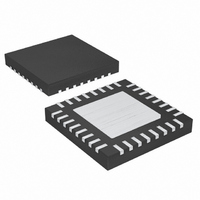
MAX17003ETJ+ Maxim Integrated Products, MAX17003ETJ+ Datasheet - Page 26

MAX17003ETJ+
Manufacturer Part Number
MAX17003ETJ+
Description
IC PS CTRLR FOR NOTEBOOKS 32TQFN
Manufacturer
Maxim Integrated Products
Datasheet
1.MAX17003ETJ.pdf
(36 pages)
Specifications of MAX17003ETJ+
Applications
Controller, Notebook Computers
Voltage - Input
6 ~ 26 V
Number Of Outputs
4
Voltage - Output
3.3V, 5V, 2 ~ 5.5 V
Operating Temperature
-40°C ~ 85°C
Mounting Type
Surface Mount
Package / Case
32-TQFN Exposed Pad
Lead Free Status / RoHS Status
Lead free / RoHS Compliant
High-Efficiency, Quad-Output, Main Power-
Supply Controllers for Notebook Computers
Ferrite cores are often the best choice, although pow-
dered iron is inexpensive and can work well at 200kHz.
The core must be large enough not to saturate at the
peak inductor current (I
A coupled inductor or transformer can be substituted
for the inductor in the 5V SMPS to create an auxiliary
output (Figure 1). The MAX17003/MAX17004 is particu-
larly well suited for such applications because the sec-
ondary feedback threshold automatically triggers DL5
even if the 5V output is lightly loaded.
The power requirements of the auxiliary supply must be
considered in the design of the main output. The trans-
former must be designed to deliver the required current
in both the primary and the secondary outputs with the
proper turns ratio and inductance. The power ratings of
the synchronous-rectifier MOSFETs and the current limit
in the MAX17003/MAX17004 must also be adjusted
accordingly. Extremes of low input-output differentials,
widely different output loading levels, and high turns
ratios can further complicate the design due to parasitic
transformer parameters such as interwinding capaci-
tance, secondary resistance, and leakage inductance.
Power from the main and secondary outputs is com-
bined to get an equivalent current referred to the main
output. Use this total current to determine the current
limit (see the Setting the Current Limit section):
where I
to the main output, and P
power from both the main output and the secondary
output:
where N is the transformer turns ratio, V
mum required rectified secondary voltage, V
forward drop across the secondary rectifier, V
is the minimum value of the main output voltage, and
V
nous-rectifier MOSFET. The transformer secondary
return is often connected to the main output voltage
26
RECT
MAX17003/MAX17004 Auxiliary Output)
______________________________________________________________________________________
is the on-state voltage drop across the synchro-
TOTAL
I
PEAK
N
=
is the equivalent output current referred
I
TOTAL
V
=
OUT
I
LOAD MAX
5
V
= P
PEAK
+
SEC
(
Transformer Design (for
TOTAL
V
RECT
TOTAL
+
):
)
V
+
FWD
is the sum of the output
Δ
+
/V
I
INDUCTOR
V
OUT5
SENSE
2
SEC
is the mini-
FWD
OUT5(MIN)
is the
instead of ground in order to reduce the necessary turns
ratio. In this case, subtract V
voltage (V
equation above. The secondary diode in coupled-induc-
tor applications must withstand flyback voltages greater
than 60V. Common silicon rectifiers, such as the 1N4001,
are also prohibited because they are too slow. Fast sili-
con rectifiers such as the MURS120 are the only choice.
The flyback voltage across the rectifier is related to the
V
turns ratio:
where N is the transformer turns ratio (secondary wind-
ings/primary windings), and V
ondary DC output voltage. If the secondary winding is
returned to V
from V
reverse breakdown voltage rating must also accommo-
date any ringing due to leakage inductance. The
diode’s current rating should be at least twice the DC
load current on the secondary output.
The inductor ripple current also impacts transient-
response performance, especially at low V
ferentials. Low inductor values allow the inductor
current to slew faster, replenishing charge removed
from the output filter capacitors by a sudden load step.
The total output voltage sag is the sum of the voltage
sag while the inductor is ramping up, and the voltage
sag before the next pulse can occur:
where D
Characteristics ), T is the switching period (1/f
ΔT equals V
I
overshoot during a full-load to no-load transient due to
stored inductor energy can be calculated as:
MAX
IN
- V
/(V
FLYBACK
OUT5
IN
V
MAX
V
SAG
FLYBACK
- V
SEC
OUT
is maximum duty factor (see the Electrical
difference, according to the transformer
OUT
OUT5
=
V
SOAR
- V
/V
2
Δ
in the equation above. The diode’s
C
IN
) when in skip mode. The amount of
I
OUT5
LOAD MAX
OUT IN
= V
instead of ground, subtract V
x T when in PWM mode, or L x 0.2 x
≈
L I
SEC
(
(
(
) in the transformer turns-ratio
Δ
V
(
Δ
C
I
2
LOAD MAX
LOAD MAX
OUT
C
+ (V
x D
OUT OUT
)
(
OUT5
Transient Response
SEC
T
(
(
MAX
IN
−
V
– V
Δ
is the maximum sec-
T
)
from the secondary
)
−
)
)
)
OUT5
2
2
V
L
OUT
) x N
IN
)
+
- V
OSC
OUT
), and
OUT5
dif-


