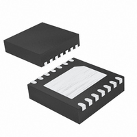
MAX8620YETD+T Maxim Integrated Products, MAX8620YETD+T Datasheet - Page 15

MAX8620YETD+T
Manufacturer Part Number
MAX8620YETD+T
Description
IC UPMIC FOR MPU 14-TDFN
Manufacturer
Maxim Integrated Products
Datasheet
1.MAX8620YETDT.pdf
(18 pages)
Specifications of MAX8620YETD+T
Applications
Micro-Power Management Integrated Circuit (UPMIC), DSPs
Voltage - Input
2.7 ~ 5.5 V
Number Of Outputs
3
Voltage - Output
0.6 ~ 3.3 V
Operating Temperature
-40°C ~ 85°C
Mounting Type
Surface Mount
Package / Case
14-TDFN Exposed Pad
Mounting Style
SMD/SMT
Maximum Operating Temperature
+ 85 C
Minimum Operating Temperature
- 45 C
Output Current
500 mA
Output Voltage
0.6 V to 3.3 V
Supply Current
115 uA
Lead Free Status / RoHS Status
Lead free / RoHS Compliant
The output capacitor, C
output voltage ripple small and to ensure regulation
loop stability. C
switching frequency. Ceramic capacitors with X5R or
X7R dielectric are highly recommended due to their
small size, low ESR, and small temperature coefficients.
Due to the unique feedback network, the output capac-
itance can be very low. For most applications, a 2.2µF
capacitor is sufficient. For optimum load-transient per-
formance and very low output ripple, the output capaci-
tor value in µFs should be equal to or larger than the
inductor value in µHs.
The input capacitor, C
drawn from the battery or input power source and
reduces switching noise in the IC. The impedance of
C
Ceramic capacitors with X5R or X7R dielectrics are
highly recommended due to their small size, low ESR,
and small temperature coefficients. Use a 10µF ceram-
ic capacitor or equivalent amount of multiple capacitors
in parallel between IN1 and GND. Connect C
close as possible to the MAX8620Y to minimize the
impact of PC board trace inductance.
The feed-forward capacitor, C
loop response, controls the switching frequency, and is
critical in obtaining the best efficiency possible.
Choose a small ceramic C0G (NPO) or X7R capacitor
with a value given by:
where R1 is the resistor between LX and FB (Figure 2).
Select the closest standard value to C
For applications that require greater than 150mA of out-
put current, connect a 4.7µF ceramic capacitor
between the LDO output and GND. For applications
that require less than 150mA of output current, connect
a 2.2µF ceramic capacitor between the LDO output
and GND. The LDO output capacitor’s (C
IN
at the switching frequency should be kept very low.
Step-Down Converter Output Capacitor
OUT3
______________________________________________________________________________________
C
must have low impedance at the
FF
IN
OUT3
=
, reduces the current peaks
R
L
1
×
Feed-Forward Capacitor
Capacitor Selection
, is required to keep the
µPMIC for Microprocessors or DSPs
LDO Output Capacitors
10
FF
S
, sets the feedback
FF
Input Capacitor
as possible.
OUT_
) equiva-
IN
as
lent series resistance (ESR) affects stability and output
noise. Use output capacitors with an ESR of 0.1Ω or
less to ensure stability and optimum transient response.
Surface-mount ceramic capacitors have very low ESR
and are commonly available in values up to 10µF.
Connect C
to minimize the impact of PC board trace inductance.
The MAX8620Y total power dissipation, P
ed using the following equations:
where P
step-down converter efficiency, and R
the inductor’s DC resistance.
The die junction temperature can be calculated as follows:
where θ
T
ditions.
High switching frequencies and relatively large peak
currents make the PC board layout a very important
aspect of design. Good design minimizes excessive
EMI on the feedback paths and voltage gradients in the
ground plane, both of which can result in instability or
regulation errors. Connect C
Connect the inductor and output capacitors (C
close to the IC as possible and keep the traces short,
direct, and wide.
The traces between C
to inductor magnetic-field interference. Route these
traces between ground planes or keep the traces away
from the inductor.
`
J
in Portable Equipment
P
should not exceed +150°C in normal operating con-
D
P
LOSS OUT
=
JA
IN(OUT3)
P
P
LOSS OUT
P
(
LOSS OUT
= 55°C/W at +70°C.
OUT
LOSS OUT
(
3
Power Dissipation and Thermal
(
T
as close as possible to the MAX8620Y
(
)
J
is the input power for OUT3, η is the
PC Board Layout and Routing
=
×
=
1
1
)
)
2
P
R
)
IN OUT
+
T
OUT3
DC
=
=
A
(
P
( (
I
LOSS OUT
I
(
INDUCTOR
(
+
OUT
OUT
, C
3
P
IN
)
⎛
⎜
⎝
D
1
(
2
FF
1
)
)
close to IN1 and GND.
(
(
V
, and FB are sensitive
−
× θ
V
IN
IN
100
2
)
Considerations
)
η
−
−
JA
+
V
DC(INDUCTOR)
⎞
⎟
⎠
V
OUT
OUT
P
−
LOSS OUT
D
I
2
, is estimat-
(
1
OUT
)
)
(
OUT3
3
)
2
3
) as
)
15
is


