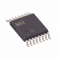
MAX3353EEUE+T Maxim Integrated Products, MAX3353EEUE+T Datasheet - Page 4

MAX3353EEUE+T
Manufacturer Part Number
MAX3353EEUE+T
Description
IC CHARGE PUMP USB OTG 16TSSOP
Manufacturer
Maxim Integrated Products
Datasheet
1.MAX3353EEUET.pdf
(21 pages)
Specifications of MAX3353EEUE+T
Applications
Charge Pump, USB
Voltage - Input
2.6 ~ 5.5 V
Number Of Outputs
2
Operating Temperature
-40°C ~ 85°C
Mounting Type
Surface Mount
Package / Case
16-TSSOP
Maximum Operating Temperature
+ 85 C
Mounting Style
SMD/SMT
Minimum Operating Temperature
- 40 C
Lead Free Status / RoHS Status
Lead free / RoHS Compliant
Voltage - Output
-
Lead Free Status / Rohs Status
Lead free / RoHS Compliant
USB On-the-Go Charge Pump with Switchable
Pullup/Pulldown Resistors
ELECTRICAL CHARACTERISTICS (continued)
(V
V
values are at V
TIMING CHARACTERISTICS
(V
V
ues are at T
4
Time to Assert D+ Pullup
Time to Assert SE0
Interrupt Propagation Delay
V
INT Out Rise Time
Hysteresis Voltage
Output Voltage Low
(D+ and D- in SE0 state)
PULLUP/PULLDOWN RESISTOR SPECIFICATIONS (D+, D-, ID_IN)
Pulldown Resistor on D+
Pulldown Resistor on D-
Pullup Resistor on D+
Pullup Resistor on D-
D- Leakage Current
D+ Leakage Current
Input Impedance on D+/D-
ID_IN Pullup Resistor
ID_IN Input Voltage Low
ID_IN Input Voltage High
TRM
TRM
CC
CC
BUS
_______________________________________________________________________________________
= +2.6V to +5.5V, V
= +2.6V to +5.5V, V
and V
and V
Rise Time
PARAMETER
PARAMETER
L
A
L
decoupled with 0.1µF capacitor to ground. C
= +25°C, V
decoupled with 0.1µF capacitor to ground; C
CC
= +4V, V
CC
L
L
L
= +1.65V to V
= +1.65V to V
= +4V, V
= +1.8V, V
SYMBOL
L
SYMBOL
= +1.8V, V
V
TRM
HYST
CC
CC
= +3.3V, and T
, V
, V
TRM
TRM
I
D P _P U LLD WN = 1, D P _P U LLU P = 0,
BD IS C _AC ON N = 0
D M _P U LLD WN = 1, D M _P U LLU P = 0,
BD IS C _AC ON N = 0
D P _P U LLD WN = 0, D P _P U LLU P = 1,
BD IS C _AC ON N = 0
D M _P U LLD WN = 0, D M _P U LLU P = 1,
D P _P U LLU P = 0, BDIS C _AC ONN = 0
D M _P U LLD WN = 0, D M _P U LLU P = 0,
BD IS C _AC ON N = 0
D P _P U LLD WN = 0, D P _P U LLU P = 0,
BD IS C _AC ON N = 0
D P _P U LLU P = 0, D P _PU LLDWN = 0,
D M _P U LLU P = 0, D M _PU LLDWN = 0,
BD IS C _AC ON N = 0
TRM
SINK
BDISC_ACONN = 1, ID_IN = GND
(A Device)
BDISC_ACONN = 1,
ID_IN = floating (B Device)
(Note 6)
From 0 to 4.4V; C
V
INT out push/pull configured,
C
BUS_DRV
LOAD
= +3V to +3.6V, C
= +3V to +3.6V, C
= +3.3V.) (Notes 3, 4)
= -2.4mA
= 50pF
A
VBUS
= 1
VBUS
= +25°C.) (Notes 3, 4)
= 1µF (min), T
CONDITION
CONDITION
= 1µF (min), T
LOAD
FLYING
FLYING
= 1µF; I
= 0.1µF, V
= 0.1µF, V
A
VBUS
= T
A
= T
MIN
= 8mA;
MIN
to T
CC
CC
to T
decoupled with 1µF capacitor to ground.
decoupled with 1µF capacitor to ground;
MAX
MAX
, unless otherwise noted. Typical val-
0.025
0.67 x V
14.25
14.25
1.425
1.425
MIN
MIN
300
140
, unless otherwise noted. Typical
CC
0.061
TYP
TYP
200
0.2
20
0.33 x V
15.75
15.75
1.575
1.575
MAX
MAX
100
270
0.3
±1
±1
1
1
1
CC
UNITS
UNITS
ms
ms
ms
kΩ
kΩ
kΩ
kΩ
µA
µA
kΩ
kΩ
µs
ns
V
V
V
V


