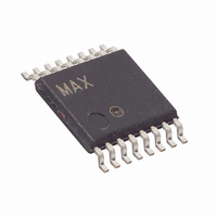
MAX3353EEUE+T Maxim Integrated Products, MAX3353EEUE+T Datasheet - Page 10

MAX3353EEUE+T
Manufacturer Part Number
MAX3353EEUE+T
Description
IC CHARGE PUMP USB OTG 16TSSOP
Manufacturer
Maxim Integrated Products
Datasheet
1.MAX3353EEUET.pdf
(21 pages)
Specifications of MAX3353EEUE+T
Applications
Charge Pump, USB
Voltage - Input
2.6 ~ 5.5 V
Number Of Outputs
2
Operating Temperature
-40°C ~ 85°C
Mounting Type
Surface Mount
Package / Case
16-TSSOP
Maximum Operating Temperature
+ 85 C
Mounting Style
SMD/SMT
Minimum Operating Temperature
- 40 C
Lead Free Status / RoHS Status
Lead free / RoHS Compliant
Voltage - Output
-
Lead Free Status / Rohs Status
Lead free / RoHS Compliant
The MAX3353E also has a special feature that allows it
to control the timing of the V
Since an OTG device could be plugged into a PC, the
V
damage to a PC host. For this reason, V
done by turning on and off a current source. The V
pulse must be timed so it drives a 13µF load (when it is
connected to the A Device) to a voltage greater than
2.1V, and it drives a >96µF load (when it is connected to
a standard PC) to a voltage less than 2.0V.
Firmware can control the current source and the timing
of the V
The MAX3353E also has the capability to time the pulse
USB On-the-Go Charge Pump with Switchable
Pullup/Pulldown Resistors
Figure 3. Pullup and Pulldown Resistors Network
Figure 4. 2-Wire Serial Interface Timing Details
10
BUS
SDA
SCL
(POWER ON)
DEFAULT
VALUES
______________________________________________________________________________________
pulse must be particularly well controlled to prevent
15kΩ
SW4
BUS
7
0
(POWER-ON) POSITIONS. A "1" CLOSES A SWITCH.
NOTE: SWITCHES ARE SHOWN IN THEIR DEFAULT
t
HD:STA
pulse through the V
6
0
SW3
15kΩ
1.5kΩ
5
0
t
F
CONTROL REGISTER 1
SW2
V
TRM
4
0
BUS
3
0
SW1
t
LOW
pulse.
BIT 4
BUS_CHG2
1
1
0
0
2
0
BIT 5
t
0
1
0
1
SU:DAT
1
0
BUS
CLOSED
CLOSED
OPEN
OPEN
SW1
0
0
control bit.
t
R
D+
D-
GND
pulsing is
CLOSED
OPEN
OPEN
OPEN
SW2
BUS
t
HIGH
itself. Firmware initiates the self-timed V
setting the V
The internal timer and current generator guarantee that
the V
within 90ms and stands below 2.0V if C
Once the time has elapsed, if another V
required, it is necessary to clear the V
then set it again.
Note: SRP V
erator work only if the MAX3353E is not in shutdown.
For OTG operation, D+ and D- are connected to switch-
able pulldown resistors (host) and switchable pullup
resistors (peripheral). Data-line pullup/pulldown resistors
are individually controlled through data bits 4 through 7 in
control register 1. Two 15kΩ pulldown resistors allow the
device to be set as a host and are asserted by bits 6 and
7. The 1.5kΩ pullup resistor is applied to the data lines
through SW1 and SW2, which are controlled by bits 4 and
5. D+ pullup has higher priority to avoid direct connection
of D+ and D-. Each of the control bits controls a designat-
ed switch; therefore, pullup and pulldown switches can
be asserted at the same time. A simplified schematic of
the switching network is shown in Figure 3.
The bidirectional D+ and D- lines are ESD protected to
±15kV, reducing external components in many applications.
A register file that interfaces to the control logic uses a
simple 2-wire interface operating up to 400kHz to con-
trol the various switches and modes.
The MAX3353E operates as a slave that sends and
receives control and status signals through an I
compatible 2-wire interface. The interface uses a serial
data line (SDA) and a serial clock line (SCL) to achieve
Data-Line Pullup and Pulldown Resistance
BUS
2-Wire I
t
HD:DAT
voltage goes above 2.1V if C
BUS_CHG1
BUS
Applications Information
2
pulsing and its associated current gen-
C-Compatible Serial Interface
control bit to 1.
t
SU:STO
Serial Addressing
BUS_CHG1
VBUS
BUS
VBUS
t
BUS
BUF
pulse by
pulse is
> 96µF.
< 13µF
bit and
2
C-


