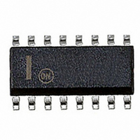
CS5165AGDWR16G ON Semiconductor, CS5165AGDWR16G Datasheet - Page 14

CS5165AGDWR16G
Manufacturer Part Number
CS5165AGDWR16G
Description
IC CTRLR BUCK SYNC 5BIT 16-SOIC
Manufacturer
ON Semiconductor
Datasheet
1.CS5165AGDWR16G.pdf
(18 pages)
Specifications of CS5165AGDWR16G
Applications
Controller, Intel Pentium® II
Voltage - Input
8 ~ 14 V
Number Of Outputs
2
Voltage - Output
1.34 ~ 2.09 V, 2.14 ~ 3.54 V
Operating Temperature
0°C ~ 70°C
Mounting Type
Surface Mount
Package / Case
16-SOIC (0.300", 7.5mm Width)
Mounting Style
SMD/SMT
Lead Free Status / RoHS Status
Lead free / RoHS Compliant
Available stocks
Company
Part Number
Manufacturer
Quantity
Price
Part Number:
CS5165AGDWR16G
Manufacturer:
ON/安森美
Quantity:
20 000
NFET conduction times by guaranteeing a typical 65 ns
non−overlap between the upper and lower MOSFET gate drive
pulses. This feature eliminates the potentially catastrophic
effect of “shoot−through current”, a condition during which
both FETs conduct causing them to overheat, self−destruct, and
possibly inflict irreversible damage to the processor.
which effects regulator efficiency and FET thermal
management requirements.
follows:
Off Time Capacitor (C
to calculate the regulator switching frequency and select the
C
where:
Figure 27. Normal Operation Showing the Guaranteed
OFF
Non−Overlap Time Between the High and Low−Side
Trace 1 = GATE(H) (5.0 V/div.)
Trace 2 = GATE(L) (5.0 V/div.)
The CS5165A provides adaptive control of the external
The most important aspect of FET performance is RDS
The power dissipated by the MOSFETs may be estimated as
Switching MOSFET:
Synchronous MOSFET:
Duty Cycle =
The C
The preceding equations for duty cycle can also be used
Power + I LOAD 2
timing capacitor:
V OUT ) (I LOAD
Power + I LOAD 2
V IN )(I LOAD
* (I LOAD
OFF
C OFF +
MOSFET Gate Drives, I
timing capacitor sets the regulator off time:
Period +
T OFF + C OFF
Perioid
RDS ON OF SWITCH FET )
OFF
switching frequency
RDS ON OF SYNCH FET )
RDS ON
RDS ON OF SYNCH FET )
)
RDS ON
4848.5
( 1 * duty cycle )
1
LOAD
4848.5
( 1 * duty cycle )
duty cycle
= 14 A
@ 2.2 V
http://onsemi.com
ON
CS5165A
,
14
Power + V BD
Schottky Diode for Synchronous FET
in parallel with the synchronous FET to conduct the inductor
current upon turn off of the switching FET to improve
efficiency. The CS5165A reference circuit does not use this
device due to it’s excellent design. Instead, the body diode of
the synchronous FET is utilized to reduce cost and conducts the
inductor current. For a design operating at 200 kHz or so, the
low non−overlap time combined with Schottky forward
recovery time may make the benefits of this device not worth
the additional expense. The power dissipation in the
synchronous MOSFET due to body diode conduction can be
estimated by the following equation:
diode. For the CS5165A demonstration board:
“Droop” Resistor for Adaptive Voltage Positioning
voltage within specification during load transients. To
implement adaptive voltage positioning a “Droop Resistor”
must be connected between the output inductor and output
capacitors and load. This resistor carries the full load current
and should be chosen so that both DC and AC tolerance limits
are met. An embedded PC trace resistor has the distinct
advantage of near zero cost implementation. However, this
droop resistor can vary due to three reasons: 1) the sheet
resistivity variation causes the thickness of the PCB layer to
vary. 2) the mismatch of L/W, and 3) temperature variation.
Power + 1.6 V
For synchronous operation, a Schottky diode may be placed
Where V
This is only 1.1% of the 40 W being delivered to the load.
Adaptive voltage positioning is used to help keep the output
where:
R
T = operating temperature
R = desired droop resistor value
For temperature T = 50°C, the % R change = 12%
a + 0.00393
1. Sheet Resistivity for one ounce copper, the thickness
2. Mismatch due to L/W. The variation in L/W is
3. Thermal Considerations. Due to I
20
variation typically 1.15 mil to 1.35 mil. Therefore the
error due to sheet resistivity is:
governed by variations due to the PCB manufacturing
process that affect the geometry and the power
dissipation capability of the droop resistor. The error
due to L/W mismatch is typically 1.0%.
the surface temperature of the droop resistor will
increase causing the resistance to increase. Also, the
ambient temperature variation will contribute to the
increase of the resistance, according to the formula:
= resistance at 20°C
°C
BD
= the forward drop of the MOSFET body
I LOAD
R + R 20 [1 ) a 20 (T * 20)]
1.35 * 1.15
14.2 A
1.25
conduction time
100 ns
+ 16%
200 kHz + 0.45 W
2
switching frequency
× R power losses


