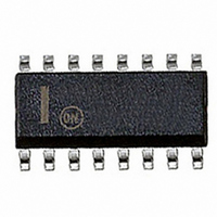
CS5165AGDWR16G ON Semiconductor, CS5165AGDWR16G Datasheet - Page 13

CS5165AGDWR16G
Manufacturer Part Number
CS5165AGDWR16G
Description
IC CTRLR BUCK SYNC 5BIT 16-SOIC
Manufacturer
ON Semiconductor
Datasheet
1.CS5165AGDWR16G.pdf
(18 pages)
Specifications of CS5165AGDWR16G
Applications
Controller, Intel Pentium® II
Voltage - Input
8 ~ 14 V
Number Of Outputs
2
Voltage - Output
1.34 ~ 2.09 V, 2.14 ~ 3.54 V
Operating Temperature
0°C ~ 70°C
Mounting Type
Surface Mount
Package / Case
16-SOIC (0.300", 7.5mm Width)
Mounting Style
SMD/SMT
Lead Free Status / RoHS Status
Lead free / RoHS Compliant
Available stocks
Company
Part Number
Manufacturer
Quantity
Price
Part Number:
CS5165AGDWR16G
Manufacturer:
ON/安森美
Quantity:
20 000
output voltage V
Power Good from interrupting the CPU unnecessarily, the
CS5165A has a built−in delay to prevent noise at the V
from toggling Power Good. The internal time delay is designed
to take about 75 ms for Power Good to go low and 65 ms for it
to recover. This allows the Power Good signal to be completely
insensitive to out of regulation conditions that are present for
a duration less than the built in delay (see Figure 25).
of regulation or in regulation level for at least the built−in delay
time duration before the Power Good signal can change state.
Figure 24 shows the relationship between the regulated
It is therefore required that the output voltage attains an out
Figure 25. Power Good is Insensitive to Out of
Trace 2− PWRGD (2.0 V/div.)
Trace 4− V
Trace 2− PWRGD (2.0 V/div.)
Trace 4− V
Figure 24. Power Good Response to an Out of
Regulation Conditions that are Present for a
Duration Less Than the Built In Delay
FB
FB
(1.0 V/div.)
(1.0 V/div.)
FB
Regulation Condition
and the Power Good signal. To prevent
http://onsemi.com
FB
pin
CS5165A
13
Selecting External Components
of external power components to optimize the cost and
performance of a particular design. The following information
can be used as general guidelines to assist in their selection.
NFET Power Transistors
reference designs derive gate drive from the 12 V supply
which is generally available in most computer systems and
utilize logic level FETs. A charge pump may be easily
implemented to support 5.0 V only systems. Multiple FET’s
may be paralleled to reduce losses and improve efficiency and
thermal management.
circuit used. Both upper and lower gate driver outputs are
specified to drive to within 1.5 V of ground when in the low
state and to within 2.0 V of their respective bias supplies when
in the high state. In practice, the FET gates will be driven rail
to rail due to overshoot caused by the capacitive load they
present to the controller IC. For the typical application where
V
output current, the following gate drive is provided:
CC
The CS5165A buck regulator can be used with a wide range
Both logic level and standard FETs can be used. The
Voltage applied to the FET gates depends on the application
(see Figure 26)
Figure 26. Gate Drive Waveforms Depicting
= 12 V and 5.0 V is used as the source for the regulator
Trace 3− GATE(H) (10 V/div.)
Trace 1− GATE(H) − 5.0 V
Trace 4− GATE(L) (10 V/div.)
Trace 2− Inductor Switching Node (5.0 V/div.)
V GS(TOP) + 12 V * 5.0 V + 7.0 V
V GS(BOTTOM) + 12 V
Rail to Rail Swing
IN


