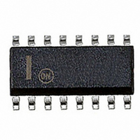
CS5165AGDWR16G ON Semiconductor, CS5165AGDWR16G Datasheet

CS5165AGDWR16G
Specifications of CS5165AGDWR16G
Available stocks
Related parts for CS5165AGDWR16G
CS5165AGDWR16G Summary of contents
Page 1
... Package CS5165AGDW16 SOIC−16 CS5165AGDW16G SOIC−16 (Pb−Free) CS5165AGDWR16 SOIC−16 1000/Tape & Reel CS5165AGDWR16G SOIC−16 (Pb−Free) †For information on tape and reel specifications, including part orientation and tape sizes, please refer to our Tape and Reel Packaging Specifications Brochure, BRD8011/D. 1 MARKING ...
Page 2
SS 0.1 mF COMP GATE(H) C OFF GATE(L) 330 pF 0 ID4 PGND V ID3 LGND V ID2 CS5165A V ID1 PWRGD V ID0 ENABLE Figure 1. Application Diagram 14.2 A for ...
Page 3
ELECTRICAL CHARACTERISTICS (0°C < ID4 ID2 ID1 ID0 ID3 ; GATE(H) Characteristic V Supply Current CC Operating 1.0 V < Loads on GATE(H) and ...
Page 4
ELECTRICAL CHARACTERISTICS ( ID4 ID2 ID1 ID0 ID3 ; Characteristic Enable Input Pullup Current ENABLE = 0 V Pullup Voltage No load on ENABLE pin Input Resistance ENABLE ...
Page 5
ELECTRICAL CHARACTERISTICS (0°C < ID4 ID2 ID1 ID0 ID3 ; GATE(H) Characteristic Voltage Identification DAC ...
Page 6
PACKAGE PIN DESCRIPTION PACKAGE PIN # SOIC−16 PIN SYMBOL −V Voltage ID DAC input pins. These pins are internally pulled left open. V ID0 ID4 the DAC range. When ...
Page 7
TYPICAL PERFORMANCE CHARACTERISTICS 200 180 160 140 120 100 2000 4000 6000 8000 10000 12000 14000 16000 Load Capacitance (pF) Figure 3. GATE(L) Risetime vs. Load Capacitance 200 180 160 140 120 100 80 ...
Page 8
THEORY OF OPERATION 2 V Control Method 2 The V method of control uses a ramp signal that is generated by the ESR of the output capacitors. This ramp is proportional to the AC current through the main inductor and ...
Page 9
The GATE(H) output will remain on, enabling the NFET switch, until terminated by either the PWM comparator, or the maximum on time timer. If the maximum on time is exceeded before the regulator output voltage achieves the ...
Page 10
Trace 1− GATE(H) (10 V/div.) Trace 2− Inductor Switching Node (5.0 V/div.) Trace 3− Output Inductor Ripple Current (2.0 A/div.) Trace 4− V ripple (20 mV/div.) OUT Figure 13. Normal Operation Showing Output Inductor Ripple Current and Output Voltage Ripple, ...
Page 11
Trace 1− GATE(H) (10 V/div.) Trace 2− Inductor Switching Node (5.0 V/div.) Trace 3− Load Current (5.0 A/div) Trace 4− V (100 mV/div.) OUT Figure 17. Output Voltage Transient Response Load Turn−Off +2.84 V ...
Page 12
The bottom FET and board trace must be properly designed to implement the OVP function.If a dedicated OVP output is required, it can be ...
Page 13
Trace 2− PWRGD (2.0 V/div.) Trace 4− V (1.0 V/div.) FB Figure 24. Power Good Response to an Out of Regulation Condition Figure 24 shows the relationship between the regulated output voltage V and the Power Good signal. To prevent ...
Page 14
Trace 1 = GATE(H) (5.0 V/div.) Trace 2 = GATE(L) (5.0 V/div.) Figure 27. Normal Operation Showing the Guaranteed Non−Overlap Time Between the High and Low−Side MOSFET Gate Drives, I LOAD The CS5165A provides adaptive control of the external NFET ...
Page 15
Droop Resistor Tolerance Tolerance due to sheet resistivity variation Tolerance due to L/W error Tolerance due to temperature variation Total tolerance for droop resistor In order to determine the droop resistor value the nominal voltage drop across it at full ...
Page 16
This applies for current spikes that are faster than regulator response time. Printed Circuit Board resistance will add to the ESR of the output capacitors. In order to limit spikes to 100 mV for a 14.2 A Load Step, ESR ...
Page 17
Rapid changes in voltage across parasitic capacitors and abrupt changes in current in parasitic inductors are major concerns for a good layout. 2. Keep high currents out of logic grounds. 3. Avoid ground loops as they pick up noise. ...
Page 18
... SOIC−16WB Typical 23 Typical 105 N. American Technical Support: 800−282−9855 Toll Free USA/Canada Japan: ON Semiconductor, Japan Customer Focus Center 2−9−1 Kamimeguro, Meguro−ku, Tokyo, Japan 153−0051 Phone: 81−3−5773−3850 http://onsemi.com 18 NOTES: 1. DIMENSIONS ARE IN MILLIMETERS. 2. INTERPRET DIMENSIONS AND TOLERANCES PER ASME Y14 ...


