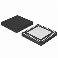
NCP4200MNR2G ON Semiconductor, NCP4200MNR2G Datasheet - Page 11

NCP4200MNR2G
Manufacturer Part Number
NCP4200MNR2G
Description
IC CONV SYNC BUCK PMBUS 40QFN
Manufacturer
ON Semiconductor
Datasheet
1.NCP4200MNR2G.pdf
(32 pages)
Specifications of NCP4200MNR2G
Applications
Converter, Intel VR11, VR11.1
Voltage - Input
1.7 ~ 24 V
Number Of Outputs
1
Voltage - Output
0.375 ~ 1.8 V
Operating Temperature
0°C ~ 85°C
Mounting Type
Surface Mount
Package / Case
40-VFQFN Exposed Pad
Output Voltage
0.375 V to 1.6 V
Output Current
500 uA
Input Voltage
1.7 V to 24 V
Switching Frequency
0.25 MHz to 6 MHz
Operating Temperature Range
0 C to + 85 C
Mounting Style
SMD/SMT
Duty Cycle (max)
100 %
Isolated/non-isolated
Non Isolated
Lead Free Status / RoHS Status
Lead free / RoHS Compliant
Available stocks
Company
Part Number
Manufacturer
Quantity
Price
Company:
Part Number:
NCP4200MNR2G
Manufacturer:
PHILIPS
Quantity:
124
Description
Interface. A typical application circuit is shown in Figure 2.
Startup Sequence
Figure 7. After both the EN and UVLO conditions are met,
a programmable internal timer goes through one delay cycle
TD1. This delay cycle is programmed using Delay
Command, default delay = 2 ms, see Table 2 for
programmable values. The first six clock cycles of TD2 are
blanked from the PWM outputs and used for phase detection
as explained in the following section. Then the
programmable internal soft−start ramp is enabled (TD2) and
the output comes up to the boot voltage of 1.1 V. The boot
hold time is also set by Delay Command. This second delay
cycle is called TD3. During TD3 the processor VID pins
settle to the required VID code. When TD3 is over, the
NCP4200 reads the VID inputs and soft−starts either up or
down to the final VID voltage (TD4). After TD4 has been
completed and the PWRGD masking time (equal to VID
OTF masking) is finished, a third cycle of the internal timer
sets the PWRGD blanking (TD5).
using the serial interface, the Delay Command and the
Soft−Start Commands.
Internal Delay Timer
sequence, TD1, TD3 and TD5. The default time is 2 msec,
which can be changed using the I
used for multiple delay timings (TD1, TD3 and TD5) during
the startup sequence. Also, it is used for timing the current
(NCP4200 PWRGD)
The NCP4200 is a 4 Phase DC−DC regulator with an I
The NCP4200 follows the startup sequence shown in
The internal delay and soft−start times are programmable
An internal timer sets the delay times for the start up
(NCP4200 EN)
VCC_CORE
VID INPUTS
VR READY
SUPPLY
VTT I/O
5.0 V
CPU
Figure 7. Startup Sequence
UVLO
THRESHOLD
VID INVALID
0.85 V
TD1
TD2
2
C interface. This timer is
50 m
V
(1.1 V)
TD3
BOOT
s
V
VID
VID VALID
TD4
TD5
http://onsemi.com
2
C
11
limit latchoff as explained in the Current Limit section. The
current limit timer is set to 4 times the delay timer.
Ton Delay command (0xD4). The delay can be programmed
between 0.5 msec and 4 msec. Table 1 provides the
programmable delay times.
Soft−Start
internal timer. The default value is 0.5 V/msec, which can be
programmed through the I
phase detection cycle have been completed, the SS time
(TD2 in Figure 2) starts. The SS circuit uses the internal VID
DAC to increase the output voltage in 6.25 mV steps up to
the 1.1 V boot voltage.
voltage delay time (TD3) is started. The end of the boot
voltage delay time signals the beginning of the second
soft−start time (TD4). The SS voltage changes from the boot
voltage to the programmed VID DAC voltage (either higher
or lower) using 6.25 mV steps.
of the Ton_Rise (0xD5) command code. Table 2 provides
the soft−start values.
Table 1. Delay Codes
Table 2. Slew Rate Codes
The delay timer is programmed using Bits <2:0> of the
The Soft−Start slope for the output voltage is set by an
Once the SS circuit has reached the boot voltage, the boot
The soft−start slew rate is programmed using Bits <2:0>
Code
Code
000
001
010
011
100
101
110
000
001
010
011
100
101
110
111
111
2
C interface. After TD1 and the
Slew Rate (V/msec)
Delay (msec)
0.5 = default
2 = default
0.5
1.5
2.5
3.5
0.1
0.3
0.7
0.9
1.1
1.3
1.5
1
3
4


