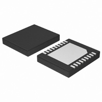
NCP5210MNR2G ON Semiconductor, NCP5210MNR2G Datasheet - Page 10

NCP5210MNR2G
Manufacturer Part Number
NCP5210MNR2G
Description
IC CTLR PWM/DDR DUAL BUCK 20-DFN
Manufacturer
ON Semiconductor
Datasheet
1.NCP5210MNR2G.pdf
(18 pages)
Specifications of NCP5210MNR2G
Applications
Controller, DDR
Voltage - Input
4.5 ~ 13.2 V
Number Of Outputs
3
Operating Temperature
0°C ~ 70°C
Mounting Type
Surface Mount
Package / Case
20-TFQFN Exposed Pad
Output Current
2 A
Switching Frequency
500 KHz
Operating Temperature Range
0 C to + 70 C
Mounting Style
SMD/SMT
Duty Cycle (max)
100 %
Lead Free Status / RoHS Status
Lead free / RoHS Compliant
Voltage - Output
-
Lead Free Status / Rohs Status
Lead free / RoHS Compliant
Other names
NCP5210MNR2G
NCP5210MNR2GOSTR
NCP5210MNR2GOSTR
Available stocks
Company
Part Number
Manufacturer
Quantity
Price
Company:
Part Number:
NCP5210MNR2G
Manufacturer:
MAXIM
Quantity:
68
Part Number:
NCP5210MNR2G
Manufacturer:
ON/安森美
Quantity:
20 000
General
Power Controller contains two high efficiency PWM
controllers and an integrated two−quadrant linear regulator.
controller with two external N−Ch FETs. The VTT
termination voltage is an integrated linear regulator with
sourcing and sinking current capability which tracks at 1/2
VDDQ. The MCH core voltage is created by the secondary
switching controller.
short circuit protection and thermal shutdown, makes this
device a total power solution for the MCH and DDR
memory system. This device is housed in a thermal
enhanced space−saving QFN−20 package.
ACPI Control Logic
supply. External control is applied to the high impedance
CMOS input labeled BUF_CUT. This signal and two
internal under voltage detectors are used to determine the
operating mode according to the state diagram in Figure 17.
and 12VATX, through 5VDUAL and BOOT pins
respectively. Two control signals, _5VDUALGD and
_BOOTGD, are asserted when the supply voltages are good.
mode to minimize the power consumption. When all three
supply voltages are good and BUF_CUT is LOW, the device
enters the S0 normal operating mode. Transition of
BUF_CUT from LOW to HIGH in S0 mode triggers the
device into S3 sleep mode. In S3 mode 12VATX supply
collapses. When BUF_CUT is deasserted the state will
change back to S0 mode. The IC can re−enter S5 mode by
removing one of the supplies during S0 mode. It should be
noted that transitions from S3 to S5 or vice versa are not
allowed. A timing diagram is shown in Figure 16.
regulators, as well as the conditions of output pins.
Internal Bandgap Voltage Reference
5VDUAL exceeds 2.7 V. Once this bandgap reference is in
regulation, an internal signal _VREFGD is asserted.
Table 1. Mode, Operation and Output Pin Condition
The NCP5210 3−In−1 PWM Dual Buck Linear DDR
The VDDQ supply is produced by a PWM switching
The inclusion of soft−start, supply undervoltage monitors,
The ACPI control logic is powered by the 5VDUAL
These UVLOs monitor the external supplies, 5VDUAL
The device is powered up initially in the S5 shutdown
Table 1 summarizes the operating states of all the
An internal bandgap reference is generated whenever
MODE
S0
S3
S5
Standby
Normal
DDQ
OFF
OPERATING CONDITIONS
Normal
VTT
H−Z
H−Z
DETAILED OPERATION DESCRIPTIONS
http://onsemi.com
Normal
MCH
OFF
OFF
NCP5210
10
S5−To−S0 Mode Power−Up Sequence
_VREFGD. Once the ACPI control is activated, the
powerup sequence starts by waking up the 5VDUAL
voltage monitor block. If the 5VDUAL supply is within the
preset levels, the BOOT under voltage monitor block is then
enabled. After 12VATX is ready and the BOOT UVLO is
asserted LOW, the ACPI control triggers this device from S5
shutdown mode into S0 normal operating mode by
activating the soft−start of DDQ switching regulator,
providing BUF_CUT remaining LOW.
interval is completed, the _INREGDDQ signal is asserted
HIGH to enable the VTT regulator as well as the V1P5
switching regulator.
DDQ Switching Regulator
rectification buck controller driving two external power
N−Ch FETs to supply up to 20 A. It employs voltage mode
fixed frequency PWM control with external compensation
switching at 250kHz
VDDQ output voltage is divided down and fed back to the
inverting input of an internal amplifier through the FBDDQ
pin to close the loop at VDDQ = VFBQ (1 + R1/R2). This
amplifier compares the feedback voltage with an internal
reference voltage of 1.190 V to generate an error signal for
the PWM comparator. This error signal is compared with a
fixed frequency RAMP waveform derived from the internal
oscillator to generate a pulse−width−modulated signal. The
PWM signal drives the external N−Ch FETs via the
TG_DDQ and BG_DDQ pins. External inductor L and
capacitor COUT1 filter the output waveform. When the IC
leaves the S5 state, the VDDQ output voltage ramps up at a
soft−start rate controlled by the capacitor at the SS pin.
When the regulation of VDDQ is detected in S0 mode,
_INREGDDQ goes HIGH to notify the control block.
to reduce the conduction loss in the external N−Ch FETs.
The ACPI control logic is enabled by the assertion of
Once the DDQ regulator is in regulation and the soft−start
In S0 mode the DDQ regulator is a switching synchronous
In S3 standby mode, the switching frequency is doubled
TGDDQ
Standby
Normal
Low
OUTPUT PIN CONDITIONS
BGDDQ
Standby
Normal
Low
13.2%. As shown in Figure 2, the
TP_1P5
Normal
Low
Low
BG_1P5
Normal
Low
Low


