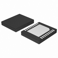
NCP5210MNR2G ON Semiconductor, NCP5210MNR2G Datasheet

NCP5210MNR2G
Specifications of NCP5210MNR2G
NCP5210MNR2GOSTR
Available stocks
Related parts for NCP5210MNR2G
NCP5210MNR2G Summary of contents
Page 1
... NOTE: Pin 21 is the thermal pad on the bottom of the device. ORDERING INFORMATION Device Package NCP5210MNR2 QFN−20 NCP5210MNR2G QFN−20 (Pb−Free) †For information on tape and reel specifications, including part orientation and tape sizes, please refer to our Tape and Reel Packaging Specification Brochure, BRD8011/D. ...
Page 2
BUF_Cut BUF_Cut CSS VTT 1.25 V, VTT 2 Apk COUT2 FBVTT AGND DDQ_REF VDDQ CZM1 CZM2 COMP_1P5 CPM1 R5 RZM2 RZM1 FB_1P5 5VDUAL R6 TG_1P5 M3 VMCH L 1 BG_1P5 COUT3 M4 GND_1P5 NCP5210 SS BOOT 5VDUAL ...
Page 3
VREF VOLTAGE and CURRENT _VREFGD REFERENCE BUF_CUT VCC _BOOTGD BOOT_ R10 UVLO VREF R11 5VDUAL 5VDUAL_ R12 UVLO R13 _5VDLGD VREF OSC S0 CSS S3 1805 Phase Shift S0 VTT Regulation Control AGND NCP5210 THERMAL SHUTDOWN TSD S0 CONTROL S3 ...
Page 4
PIN DESCRIPTION Pin Symbol 1 COMP VDDQ error amplifier compensation node. 2 FBDDQ DDQ regulator feedback pin Soft−start pin of DDQ and MCH. 4 PGND Power ground. 5 VTT VTT regulator output. 6 VDDQ Power input for VTT ...
Page 5
ELECTRICAL CHARACTERISTICS (5VDUAL = 5 V, BOOT = 12 V, 5VATX = 5 V, DDQ_REF = 2 COUT1 = 3770 mF, COUT2 = 470 mF, COUT3 = NA, CSS = 33 nF 2.166 kW ...
Page 6
ELECTRICAL CHARACTERISTICS (5VDUAL = 5 V, BOOT = 12 V, 5VATX = 5 V, DDQ_REF = 2 COUT1 = 3770 mF, COUT2 = 470 mF, COUT3 = NA, CSS = 33 nF 2.166 kW ...
Page 7
TYPICAL OPERATING CHARACTERISTICS 1.196 1.194 1.192 1.19 1.188 1.186 1.184 1.182 AMBIENT TEMPERATURE ( C) A Figure 3. VFBQ Feedback Voltage vs. Ambient Temperature 0.81 0.805 0.8 0.795 0.79 0.785 ...
Page 8
TYPICAL OPERATING WAVEFORMS Channel 2: VDDQ Output Voltage, 1.0 V/div Channel 3: VTT Output Voltage, 1.0 V/div Channel 4: V1P5 Output Voltage, 1.0 V/div Time Base: 5.0 ms/div Figure 9. Power−Up Sequence Channel 1: Current Sourced out of VTT, 2.0 ...
Page 9
TYPICAL OPERATING WAVEFORMS Channel 1: Current Sourced into of VDDQ, 10 A/div Channel 2: VDDQ Output Voltage, AC−Coupled, 100 mV/div Channel 3: VTT Output Voltage, AC−Coupled, 100 mV/div Channel 4: V1P5 Output Voltage, AC−Coupled, 100 mV/div Time Base: 1.0 ms/div ...
Page 10
General The NCP5210 3−In−1 PWM Dual Buck Linear DDR Power Controller contains two high efficiency PWM controllers and an integrated two−quadrant linear regulator. The VDDQ supply is produced by a PWM switching controller with two external N−Ch FETs. The VTT ...
Page 11
For enhanced efficiency, an active synchronous switch is used to eliminate the conduction loss contributed by the forward voltage of a diode or Schottky diode rectifier. Adaptive non−overlap timing control of the complementary gate drive output signals is provided to ...
Page 12
BUF_CUT SS pin DDQ−S0 VTT MCH State 5VSTBY or 5VSTB is the Ultimate Chip Enable. This supply has first to ensure gates ...
Page 13
BUF_CUT = 0 AND _BOOTGD = 1 NOTE: All possible state transitions are shown. All unspecified inputs do not cause any state change. Figure 17. State Transitions Diagram of NCP5210 NCP5210 S5 BUF_CUT = 0 AND (_BOOTGD = 0) S0 ...
Page 14
100 C10 R7 6 VDDQ 1 COMP Vref = 1. FBDDQ PGND VTT VDDQ 6 ...
Page 15
Application Circuit Figure 18 shows the typical application circuit for NCP5210. The NCP5210 is specifically designed as a total power solution for the MCH and DDR memory system. This diagram contains NCP5210 for driving four external N−Ch FETs to form ...
Page 16
... V 1 ECJ1VB1E333K http://onsemi.com 16 Manufacturer ON Semiconductor ON Semiconductor ON Semiconductor ON Semiconductor ON Semiconductor − − Panasonic Panasonic Panasonic Panasonic Panasonic Panasonic Panasonic Panasonic Panasonic Panasonic Panasonic Panasonic Panasonic Panasonic − − − − − − − − − − − − ...
Page 17
QFN−20, DUAL−SIDED, 6x5 PIN 1 LOCATION TOP VIEW 0. SIDE VIEW (A3 20X 20X 20X ...
Page 18
... Fax: 480−829−7709 or 800−344−3867 Toll Free USA/Canada Email: orderlit@onsemi.com NCP5210 N. American Technical Support: 800−282−9855 Toll Free USA/Canada Japan: ON Semiconductor, Japan Customer Focus Center 2−9−1 Kamimeguro, Meguro−ku, Tokyo, Japan 153−0051 Phone: 81−3−5773−3850 http://onsemi.com 18 ON Semiconductor Website: http://onsemi ...


