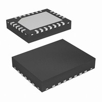
ISL8101IRZ Intersil, ISL8101IRZ Datasheet - Page 16

ISL8101IRZ
Manufacturer Part Number
ISL8101IRZ
Description
IC PWM CTRLR BUCK 2PHASE 24-QFN
Manufacturer
Intersil
Datasheet
1.ISL8101CRZ-T.pdf
(20 pages)
Specifications of ISL8101IRZ
Applications
Controller, Intel VRM9, VRM10, and AMD Hammer Applications
Voltage - Input
4.6 ~ 12 V
Number Of Outputs
1
Voltage - Output
0.6 ~ 2.3 V
Operating Temperature
-40°C ~ 85°C
Mounting Type
Surface Mount
Package / Case
24-VQFN Exposed Pad, 24-HVQFN, 24-SQFN, 24-DHVQFN
Lead Free Status / RoHS Status
Lead free / RoHS Compliant
At the beginning of the load transient, the output capacitors
supply all of the transient current. The output voltage will
initially deviate by an amount approximated by the voltage
drop across the ESL. As the load current increases, the
voltage drop across the ESR increases linearly until the load
current reaches its final value. The capacitors selected must
have sufficiently low ESL and ESR so that the total output-
voltage deviation is less than the allowable maximum.
Neglecting the contribution of inductor current and regulator
response, the output voltage initially deviates according to
Equation 21.
The filter capacitor must have sufficiently low ESL and ESR
so that ΔV < ΔV
Most capacitor solutions rely on a mixture of high-frequency
capacitors with relatively low capacitance in combination
with bulk capacitors having high capacitance but limited
high-frequency performance. Minimizing the ESL of the
high-frequency capacitors allows them to support the output
voltage as the current increases. Minimizing the ESR of the
bulk capacitors allows them to supply the increased current
with less output voltage deviation.
The ESR of the bulk capacitors is also responsible for the
majority of the output-voltage ripple. As the bulk capacitors
sink and source the inductor ac ripple current, a voltage
develops across the bulk-capacitor ESR equal to I
once the output capacitors are selected and a maximum
allowable ripple voltage, V
analysis of the available output voltage budget. Equation 22
can be used to determine a lower limit on the output
inductance.
Since the capacitors are supplying a decreasing portion of
the load current while the regulator recovers from the
transient, the capacitor voltage becomes slightly depleted.
The output inductors must be capable of assuming the entire
load current before the output voltage decreases more than
ΔV
While Equation 23 addresses the leading edge, Equation 24
gives the upper limit on L for cases where the trailing edge of
the current transient causes a greater output voltage
deviation than the leading edge.
ΔV
L
L
L
≥
≤
≤
MAX
≈
ESR
4 C V
--------------------------------
2.5 C
---------------- -
(
ΔI
(
⋅
ESL
(
⋅
)
. This places an upper limit on inductance.
ΔI
2
⋅
⋅
(
---------------------------------------------------------------- -
)
⋅
)
V
2
OUT
(
di
---- -
dt
f
IN
ΔV
S
⋅
+
–
MAX
V
⋅
(
2 V
MAX
IN
ESR
(
ΔV
⋅
⋅
–
V
OUT
MAX
.
ΔI ESR
) ΔI
P-P MAX
⋅
) V
(
–
⋅
ΔI ESR
P-P(MAX)
OUT
⋅
)
16
)
⋅
(
V
IN
)
, is determined from an
–
V
O
)
P-P
(EQ. 23)
(EQ. 21)
(EQ. 22)
(EQ. 24)
. Thus,
ISL8101
Normally, the trailing edge dictates the selection of L, since
duty cycles are usually less than 50%. Nevertheless, both
inequalities should be evaluated, and L should be selected
based on the lower of the two results. In all equations in this
paragraph, L is the per-channel inductance and C is the total
output bulk capacitance.
LAYOUT CONSIDERATIONS
MOSFETs switch very fast and efficiently. The speed with
which the current transitions from one device to another
causes voltage spikes across the interconnecting
impedances and parasitic circuit elements. These voltage
spikes can degrade efficiency, radiate noise into the circuit
and lead to device overvoltage stress. Careful component
layout and printed circuit design minimizes the voltage
spikes in the converter. Consider, as an example, the turn-off
transition of the upper PWM MOSFET. Prior to turn-off, the
upper MOSFET was carrying channel current. During the
turnoff, current stops flowing in the upper MOSFET and is
picked up by the lower MOSFET. Any inductance in the
switched current path generates a large voltage spike during
the switching interval. Careful component selection, tight
layout of the critical components, and short, wide circuit
traces minimize the magnitude of voltage spikes.
There are two sets of critical components in a DC/DC
converter using a ISL8101 controller. The power
components are the most critical because they switch large
amounts of energy. Next are small signal components that
connect to sensitive nodes or supply critical bypassing
current and signal coupling.
Note that as the ISL8101 does not allow external adjustment
of the channel-to-channel current balancing (current
information is multiplexed across a single R
is important to have a symmetrical layout, preferably with the
controller equidistantly located from the two power trains it
controls. Equally important are the gate drive lines (UGATE,
LGATE, PHASE): since they drive the power train MOSFETs
using short, high current pulses, it is important to size them
accordingly and reduce their overall impedance. Equidistant
placement of the controller to the two power trains also helps
keeping these traces equally long (equal impedances,
resulting in similar driving of both sets of MOSFETs).
The power components should be placed first. Locate the
input capacitors close to the power switches. Minimize the
length of the connections between the input capacitors, C
and the power switches. Locate the output inductors and
output capacitors between the MOSFETs and the load.
Locate the high-frequency decoupling capacitors (ceramic)
as close as practicable to the decoupling target, making use
of the shortest connection paths to any internal planes, such
as vias to GND immediately next, or even onto the capacitor
solder pad.
The critical small components include the bypass capacitors
for VCC and PVCC. Locate the bypass capacitors, C
ISEN
resistor), it
July 28, 2008
BP
FN9223.1
,
IN
,


