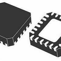
PM6641TR STMicroelectronics, PM6641TR Datasheet - Page 33

PM6641TR
Manufacturer Part Number
PM6641TR
Description
IC CTLR DDR2/3 MONO VR 48VFQFPN
Manufacturer
STMicroelectronics
Datasheet
1.PM6641TR.pdf
(47 pages)
Specifications of PM6641TR
Applications
Converter, DDR2, DDR3
Voltage - Input
2.7 ~ 5.5 V
Number Of Outputs
3
Voltage - Output
0.8 ~ 5.5 V
Operating Temperature
0°C ~ 85°C
Mounting Type
Surface Mount
Package / Case
48-VFQFN
For Use With
497-8425 - KIT EVAL PM6641 CHIPSET/DDR2/3
Lead Free Status / RoHS Status
Lead free / RoHS Compliant
Other names
497-6893-2
PM6641TR
PM6641TR
Available stocks
Company
Part Number
Manufacturer
Quantity
Price
Company:
Part Number:
PM6641TR
Manufacturer:
STM
Quantity:
35 839
PM6641
7.11
7.11.1
7.11.2
Fault management
PM6641 has been conceived to constantly monitor the rails output voltage. In order to
protect itself from failure and the load from damage, the device is able to:
●
●
●
●
●
The current limit is an auto-recovery protection, monitoring cycle by cycle the regulators
high side MOSFET current (see
details).
The output over voltage and under voltage and the input under voltage are latched
protections, whereas the thermal shutdown is auto-recovery; all these features are
described in the following sections.
Output overvoltage
If the output voltage of a switching regulator (memory supply rail VDDQ (1.8 V), chipset
supply rails 1.5 V or 1.05 V) becomes greater than 120% of its nominal value, an over
voltage (OV) protection for that rail is triggered. As a consequence the regulator stops
switching, the internal low-side power MOSFET of that rail is turned on and the high-side
MOSFET is turned off. The OV protection effect is the very quick discharge of the rail output
capacitor.
The OV condition is latched, and it can be reset only by toggling the enable pin of that rail or
by turning off and on the IC power supply (AVCC pin).
An OV condition for one of the outputs of the PM6641 has no effect on the operation of the
other outputs (e.g., if the OV protection is triggered for the VDDQ regulator, the 1.5 V and
1.05 V regulators continue to work normally).
Output under voltage
If the output voltage of a switching regulator (memory supply rail VDDQ (1.8 V), chipset
supply rails 1.5 V or 1.05 V) becomes lower than 60% of its nominal value (e.g. because the
rail was shorted to ground or the output load is increased dramatically), an under voltage
(UV) protection for that rail is triggered.
An UV condition causes the soft-end of the rail, which implies the regulator turn off and the
rail discharge MOSFET turn on (see
details); the UV condition is latched, and it can be reset only by toggling the enable pin of
that rail or by turning off and on the PM6641 power supply (AVCC pin).
As for OV protection, each switching regulator can perform under voltage protection without
affecting other regulators.
The over-current feature is implemented in the PM6641 by limiting the output current of
each rail (see
a latched UV protection if the output voltage falls because of a load requesting more current
than the limit.
Limit the power MOSFETs current
Detect output overvoltage
Detect output under voltage
Monitor the device temperature
Detect input power supply under voltage
Chapter 7.10: Peak current limit on page 31
Doc ID 13510 Rev 3
Chapter 7.10: Peak current limit on page 31
Chapter 7.7: Outputs soft-end on page 29
section for details) and triggering
Device description
section for
section for
33/47


