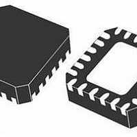
PM6641TR STMicroelectronics, PM6641TR Datasheet - Page 20

PM6641TR
Manufacturer Part Number
PM6641TR
Description
IC CTLR DDR2/3 MONO VR 48VFQFPN
Manufacturer
STMicroelectronics
Datasheet
1.PM6641TR.pdf
(47 pages)
Specifications of PM6641TR
Applications
Converter, DDR2, DDR3
Voltage - Input
2.7 ~ 5.5 V
Number Of Outputs
3
Voltage - Output
0.8 ~ 5.5 V
Operating Temperature
0°C ~ 85°C
Mounting Type
Surface Mount
Package / Case
48-VFQFN
For Use With
497-8425 - KIT EVAL PM6641 CHIPSET/DDR2/3
Lead Free Status / RoHS Status
Lead free / RoHS Compliant
Other names
497-6893-2
PM6641TR
PM6641TR
Available stocks
Company
Part Number
Manufacturer
Quantity
Price
Company:
Part Number:
PM6641TR
Manufacturer:
STM
Quantity:
35 839
Device description
7.1
7.1.1
20/47
Memory supply
The DDR2/3 section of PM6641 is based on the VDDQ rail, the VTT termination rail and the
VTTREF reference voltage buffer.
The VDDQ rail is provided by a step-down switching regulator whose output voltage, by
default, is set to 1.8 V, in order to be compliant with DDR2 JEDEC specs. The output voltage
can also be adjusted using an external resistor divider. This rail performs latched output
under-voltage and over-voltage and auto-recovery current limit, without requiring external
sensing resistor.
The VTT termination rail is supplied by a low drop-out (LDO) linear regulator, able to sink
and source up to 2 A peak current. This regulator follows the half of the VDDQ rail and is a
replica of the VTTREF reference voltage buffer. When LDOIN is directly supplied by VDDQ,
i.e. the PM6641 1S8 rail, VTT and VDDQ can perform the so called tracking discharge, in
compliance with the JEDEC specs, as described in the following section. If higher efficiency
is required, VTT can be supplied by a lower voltage rail. An output capacitor of at least 20 µF
is the only external component required.
The VTTREF reference voltage buffer is always in tracking with the half of VDDQ and is able
to sink and source up to 15 mA with an accuracy of ±2% relative to VDDQ half. A 10 nF up
to 100 nF bypass capacitor for stability purposes is required.
The VDDQ rail is provided by a constant frequency current-mode buck regulator, whose
frequency is set by inserting an external resistor between SET_SWF pin and AGND (see
Chapter 7.8: Switching frequency selection on page 29
voltage can easily be set to 1.8 V by connecting the feedback pin VFB_1S8 directly to the
output rail, avoiding the use of external components. However, if a different output voltage is
desired, the VFB_1S8 pin must be connected to the central tap of a resistor divider.
The output voltage can be adjusted from 0.8 V up to the input voltage value, decreased by a
drop due to the high-side MOSFET on resistance.
(see
The control loop needs to be compensated by inserting a resistor-capacitor series
connected between the COMP_1S8 pin and ground; if electrolytic capacitor with relevant
equivalent series resistance (ESR) are used, an additional capacitor between the
COMP_1S8 pin and ground can be useful (see
page 24
and no external components are required.
The internal high-side PMOS and low-side NMOS allow the regulator to source an average
current of 2.8 A and a peak current of 5 A. The peak current limit protection is performed by
sensing the internal high side MOSFET current and can be decreased by inserting an
external resistor between CSNS pin and AGND (see
page 31
This 1S8 rail is able to protect the load from Over-Voltage and Under-Voltage protection,
which avoid the output to be higher than 120% or lower than 60% of the nominal value (see
Chapter 7.11.1: Output overvoltage on page 33
on page 33
When the EN_1S8 pin goes high the VDDQ rail is turned on and the output voltage soft-start
is performed by slowly charging the rail output capacitor; this behavior is achieved because
VDDQ switching regulator
Chapter 7.5: Output voltage divider on page 27
section for details). The classical slope compensation is internally implemented
section for details).
section for details).
Doc ID 13510 Rev 3
Chapter 7.3: SW regulators control loop on
and
Chapter 7.11.2: Output under voltage
section for details).
Chapter 7.10: Peak current limit on
section for details). The output
PM6641


