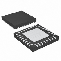
MAX17528GTJ+ Maxim Integrated Products, MAX17528GTJ+ Datasheet - Page 38

MAX17528GTJ+
Manufacturer Part Number
MAX17528GTJ+
Description
IC PWM CTRLR STP-DWN 32TQFN-EP
Manufacturer
Maxim Integrated Products
Series
Quick-PWM™r
Datasheet
1.MAX17528GTJ.pdf
(41 pages)
Specifications of MAX17528GTJ+
Applications
Controller, Intel IMVP-6.5™ GMCH
Voltage - Input
4.5 ~ 5.5 V
Number Of Outputs
1
Voltage - Output
0.01 ~ 1.5 V
Operating Temperature
-40°C ~ 105°C
Mounting Type
Surface Mount
Package / Case
32-TQFN Exposed Pad
Lead Free Status / RoHS Status
Lead free / RoHS Compliant
1-Phase Quick-PWM
Intel IMVP-6.5/GMCH Controllers
R
put capacitors and sense resistors.
For a standard 300kHz application, the ESR zero fre-
quency must be well below 95kHz, preferably below
50kHz. Tantalum, SANYO POSCAP, and Panasonic SP
capacitors in widespread use at the time of publication
have typical ESR zero frequencies below 50kHz. In the
standard GMCH application circuit, the ESR needed to
support a 10mV
Two 330µF/2.5V Panasonic SP (type SX) capacitors in
parallel provide 3.0mΩ (max) ESR. With a 5mΩ droop
and 0.5mΩ PCB resistance, the typical combined ESR
results in a zero at 28kHz.
Ceramic capacitors have a high-ESR zero frequency,
but applications with significant voltage positioning can
take advantage of their size and low ESR. Do not put
high-value ceramic capacitors directly across the out-
put without verifying that the circuit contains enough
voltage positioning and series PCB resistance to
ensure stability. When only using ceramic output
capacitors, output overshoot (V
mines the minimum output capacitance requirement.
Their relatively low capacitance value can cause output
overshoot when stepping from full-load to no-load con-
ditions, unless a small inductor value is used (high
switching frequency) to minimize the energy transferred
from inductor to capacitor during load-step recovery.
Unstable operation manifests itself in two related, but
distinctly different ways: double pulsing and feedback
loop instability. Double pulsing occurs due to noise on
the output or because the ESR is so low that there is
not enough voltage ramp in the output voltage signal.
This “fools” the error comparator into triggering a new
cycle immediately after the minimum off-time period
has expired. Double pulsing is more annoying than
harmful, resulting in nothing worse than increased out-
put ripple. However, it can indicate the possible pres-
ence of loop instability due to insufficient ESR. Loop
instability can result in oscillations at the output after
line or load steps. Such perturbations are usually
damped, but can cause the output voltage to rise
above or fall below the tolerance limits.
The easiest method for checking stability is to apply a
very fast zero-to-max load transient and carefully
observe the output voltage ripple envelope for over-
shoot and ringing. It can help to simultaneously monitor
the inductor current with an AC current probe. Do not
allow more than one cycle of ringing after the initial
step-response under/overshoot.
38
PCB
______________________________________________________________________________________
is the parasitic board resistance between the out-
P-P
ripple is 10mV/(10A x 0.3) = 3.3mΩ.
SOAR
) typically deter-
The input capacitor must meet the ripple current
requirement (I
The I
lowing equation:
The worst-case RMS current requirement occurs when
operating with V
equation simplifies to I
For most applications, nontantalum chemistries (ceramic,
aluminum, or OS-CON) are preferred due to their resis-
tance to inrush surge currents typical of systems with a
mechanical switch or connector in series with the input.
If the Quick-PWM controller is operated as the second
stage of a two-stage power-conversion system, tanta-
lum input capacitors are acceptable. In either configu-
ration, choose an input capacitor that exhibits less than
+10°C temperature rise at the RMS input current for
optimal circuit longevity.
Most of the following MOSFET guidelines focus on the
challenge of obtaining high load-current capability
when using high-voltage (> 20V) AC adapters. Low-
current applications usually require less attention.
The high-side MOSFET (N
the resistive losses plus the switching losses at both
V
Ideally, the losses at V
to losses at V
the losses at V
losses at V
(reducing R
if the losses at V
losses at V
(increasing R
over a wide range, the minimum power dissipation occurs
where the resistive losses equal the switching losses.
Choose a low-side MOSFET that has the lowest possi-
ble on-resistance (R
sized package (i.e., one or two 8-pin SOs, DPAK, or
D
DL gate driver can supply sufficient current to support
the gate charge and the current injected into the para-
sitic gate-to-drain capacitor caused by the high-side
MOSFET turning on; otherwise, cross-conduction prob-
lems can occur (see the MOSFET Gate Drivers section).
IN(MIN)
2
PAK), and is reasonably priced. Make sure that the
RMS
and V
requirements can be determined by the fol-
I
RMS
IN(MAX)
IN(MIN)
DS(ON)
DS(ON)
RMS
IN(MAX)
IN(MAX)
IN(MIN)
=
IN
IN(MAX)
⎛
⎜
⎝
) imposed by the switching currents.
I
, consider increasing the size of N
LOAD
, consider reducing the size of N
= 2 x V
but with higher C
V
to lower C
IN
, with lower losses in between. If
DS(ON)
RMS
Input Capacitor Selection
Power-MOSFET Selection
. Calculate both of these sums.
IN(MIN)
are significantly higher than the
⎞
⎟
⎠
are significantly higher than the
OUT
H
= 0.5 x I
V
) must be able to dissipate
OUT IN
), comes in a moderate-
GATE
. At this point, the above
should be roughly equal
(
V
). If V
LOAD
GATE
−
V
OUT
IN
.
). Conversely,
does not vary
)
H
H


