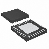
MAX17528GTJ+ Maxim Integrated Products, MAX17528GTJ+ Datasheet - Page 34

MAX17528GTJ+
Manufacturer Part Number
MAX17528GTJ+
Description
IC PWM CTRLR STP-DWN 32TQFN-EP
Manufacturer
Maxim Integrated Products
Series
Quick-PWM™r
Datasheet
1.MAX17528GTJ.pdf
(41 pages)
Specifications of MAX17528GTJ+
Applications
Controller, Intel IMVP-6.5™ GMCH
Voltage - Input
4.5 ~ 5.5 V
Number Of Outputs
1
Voltage - Output
0.01 ~ 1.5 V
Operating Temperature
-40°C ~ 105°C
Mounting Type
Surface Mount
Package / Case
32-TQFN Exposed Pad
Lead Free Status / RoHS Status
Lead free / RoHS Compliant
1-Phase Quick-PWM
Intel IMVP-6.5/GMCH Controllers
The current monitor allows the processor to accurately
monitor the CPU load and quickly calculate the power
dissipation to determine if the system is about to over-
heat before the significantly slower temperature sensor
signals an overtemperature alert.
Connect an external resistor between IMON and
VSS_SENSE to create the desired IMON gain based on
the following equation:
where IMAX is defined in the Current Monitor section of
the Intel IMVP-6.5 specification and based on discrete
increments (10A, 20A, 30A, 40A, etc.,), R
typical effective value of the current-sense element
(sense resistor or inductor DCR) that is used to provide
the current-sense voltage, and G
transconductance amplifier gain as defined in the
Electrical Characteristics table.
The IMON voltage is internally clamped to a maximum
of 1.1V (typ), preventing the IMON output from exceed-
ing the IMON voltage rating even under overload or
short-circuit conditions. When the controller is disabled,
IMON is pulled to ground.
The transconductance amplifier and voltage clamp are
internally compensated, so IMON cannot directly drive
large capacitance values. To filter the IMON signal, use
an RC filter as shown in Figure 1.
The MAX17528 also features an independent compara-
tor with an accurate threshold that tracks the analog
supply voltage (V
mal trip threshold independent of the V
age tolerance. Use a resistor- and thermistor-divider
between V
overtemperature monitor. Place the thermistor as close
as possible to the MOSFETs and inductors.
The output UVP function limits the power loss by dis-
abling the regulator if the MAX17528 output voltage
drops 400mV below the target voltage; the controller
activates the shutdown sequence and sets the fault
latch. Once the controller ramps down to zero, it forces
DL high and DH low. Toggle SHDN or cycle the V
power supply below 0.5V to clear the fault latch and
reactivate the controller.
UVP protection can be disabled through the no-fault
test mode (see the No-Fault Test Mode section).
34
______________________________________________________________________________________
R
IMON
CC
Temperature Comparator ( VRHOT )
= 0.999V/(IMAX x R
and GND to generate a voltage-regulator
Output Undervoltage (UVP) Protection
HOT
= 0.3 x V
CC
SENSE
). This makes the ther-
m(IMON)
x G
CC
m(IMON)
is the typical
SENSE
supply volt-
)
is the
CC
The MAX17528 features a thermal-fault-protection cir-
cuit. When the junction temperature rises above
+160°C, a thermal sensor sets the fault latch, forces DL
low, and pulls DH low. Toggle SHDN or cycle the V
power supply below 0.5V to clear the fault latch and
reactivate the controller after the junction temperature
cools by 15°C. Thermal shutdown can be disabled
through the no-fault test mode (see the No-Fault Test
Mode section).
The latched fault-protection feature can complicate the
process of debugging prototype breadboards since
there are (at most) a few milliseconds in which to deter-
mine what went wrong. Therefore, a “no-fault” test
mode is provided to disable the fault protection—UVP,
thermal shutdown, and TON open-circuit fault protec-
tion. The “no-fault” test mode also disables the BST
switch, although the switch’s body diode provides suffi-
cient power for the high-side driver to function properly.
Additionally, the test mode clears the fault latch if it has
been set. The no-fault test mode is entered by forcing
11V to 13V on SHDN.
The DH and DL drivers are optimized for driving mod-
erate-sized high-side and larger low-side power
MOSFETs. This is consistent with the low duty factor
seen in notebook applications, where a large V
V
source and sink 2.2A, and the low-side gate drivers
(DL) source 2.7A and sink 8A. This ensures robust gate
drive for high-current applications. The DH high-side
MOSFET driver is powered by an internal charge-pump
boost switch at BST, while the DL synchronous-rectifier
driver is powered directly by the 5V bias supply (V
Adaptive dead-time circuits monitor the DL and DH dri-
vers and prevent either FET from turning on until the
other is fully off. The adaptive driver dead time allows
operation without shoot-through with a wide range of
MOSFETs, minimizing delays and maintaining efficiency.
There must be a low-resistance, low-inductance path
from the DL and DH drivers to the MOSFET gates for
the adaptive dead-time circuits to work properly; other-
wise, the sense circuitry in the MAX17528 interprets the
MOSFET gates as “off” while charge actually remains.
Use very short, wide traces (50 mils to 100 mils wide if
the MOSFET is 1in from the driver).
OUT
differential exists. The high-side gate drivers (DH)
MOSFET Gate Drivers
Thermal Fault Protection
No-Fault Test Mode
DD
IN
CC
).
-


