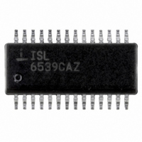
ISL6539CAZ Intersil, ISL6539CAZ Datasheet - Page 15

ISL6539CAZ
Manufacturer Part Number
ISL6539CAZ
Description
IC CTRLR DDR DRAM, SDRAM 28QSOP
Manufacturer
Intersil
Datasheet
1.ISL6539CAZ.pdf
(20 pages)
Specifications of ISL6539CAZ
Applications
Controller, DDR DRAM, SDRAM
Voltage - Input
3.3 ~ 18 V
Number Of Outputs
2
Voltage - Output
0.9 ~ 5.5 V
Operating Temperature
0°C ~ 70°C
Mounting Type
Surface Mount
Package / Case
28-QSOP
Peak Reflow Compatible (260 C)
Yes
Rohs Compliant
Yes
Lead Free Status / RoHS Status
Lead free / RoHS Compliant
Available stocks
Company
Part Number
Manufacturer
Quantity
Price
Part Number:
ISL6539CAZ
Manufacturer:
INTERSIL
Quantity:
20 000
Part Number:
ISL6539CAZ-T
Manufacturer:
INTERSIL
Quantity:
20 000
Sometimes, if the phase node is very noisy, a resistor can be
put on the ISEN pin to ground. This resistor together with the
R
internal current sense amplifier, and reduce noise coupling.
Sizing the Overcurrent Setpoint Resistor
The internal 0.9V reference is buffered to the OCSET pin
with a voltage follower (refer to the equivalent circuit in
Figure 12). The current going through the external
overcurrent set resistor is sensed from the OCSET pin. This
current, divided by 2.9, sets up the overcurrent threshold and
compares with the scaled ISEN pin current going through
R
than the threshold value, an OC signal is generated. The first
OC signal starts a counter and activates a pulse skipping
function. The inductor current will be continuously monitored
through the phase node voltage after the first OC trip. As
long as the sensed current exceeds the OC threshold value,
the following PWM pulse will be skipped. This operation will
be the same for 8 switching cycles. Another OC occurring
between 8 to 16 switching cycles would result in a latch off
with both upper and lower drives low. If there is no OC within
8 to 16 switching cycles, normal operation resumes.
Based on the previous description and the “Block Diagram” on
page 8, the OC set resistor can be calculated as Equation 17:
I
Since inductor peak current changes with input voltage, it is
better to use an oscilloscope when testing the overcurrent
setting point to monitor the inductor current, and to
determine when the OC occurs. To get consistent test results
on different boards, it is best to keep the MOSFET at a fixed
temperature.
PHASE
PHASE
R
OC
_
_
+
+
CS
CS
FIGURE 12. EQUIVALENT CIRCUIT FOR OC SIGNAL
set
Rset
Rset
is the inductor peak current and not the load current.
r
can divide the phase node voltage down, seen by the
Rdson
Rdson
with an 8µA offset. Once the sensed current is higher
DS(ON)
=
R
R
CS
CS
---------------------------------------------------
I
-------------------------------- -
OC
R
OCSET
OCSET
CS
ISEN
ISEN
r
DS ON
+
GENERATOR
10.3V
(
140
140 Ω
140 Ω
140Ω
AMPLIFIER
Amplifier
Amplifier
)
+
8μA
_
_
+
+
_
_
+
+
÷ 2.9
÷ 2.9
REFERENCE
Reference
Reference
15
0.9 V
0.9 V
÷ 33.1
÷ 33.1
+ +
+ +
Σ
Σ
8uA
8uA
8µA
I
Isense
Isense
SENSE
+
+
_
_
Comparator
Comparator
COMPARATOR
(EQ. 17)
OC
OC
ISL6539
The MOSFET will not heat-up when applying a very low
frequency and short load pulses with an electronic load to
the output.
As an example, assume the following:
• The maximum normal operation load current is 1
• The OC set point is 10% higher than the maximum load
• The inductor peak current is 1.15 to 1.3 times higher than
• The r
I
maximum load current to avoid nuisance overcurrent trip.
Selection of the LC Filter
The duty cycle of a buck converter is a function of the input
voltage and output voltage. Once an output voltage is fixed,
it can be written as Equation 18:
The switching frequency, f
peak-to-peak ripple current going through the inductor can
be written as Equation 19:
As higher ripple current will result in higher switching loss
and higher output voltage ripple, the peak-to-peak current of
the inductor is generally designed with a 20% to 40%
peak-to-peak ripple of the nominal operation current. Based
on this assumption, the inductor value can be selected with
Equation 19. In addition to the mechanical dimension, a
shielded ferrite core inductor with a very low DC resistance,
DCR, is preferred for less core loss and copper loss. The DC
copper loss of the inductor can be estimated by Equation 20:
The inductor copper loss can be significant in the total
system power loss. Attention has to be given to the DCR
selection. Another factor to consider when choosing the
inductor is its saturation characteristics at elevated
temperature. Saturated inductors could result in nuisance
OC, or OV trip.
Output voltage ripple and the transient voltage deviation are
factors that have to be taken into consideration when
selecting an output capacitor. In addition to high frequency
noise related MOSFET turn-on and turn-off, the output voltage
ripple includes the capacitance voltage drop and ESR voltage
P
OC
D V
I
P P
copper
(
current
the load current, depending on the inductor value and the
input voltage
–
should set at least 1.8 to 2 times higher than the
IN
=
)
DS(ON)
=
V
------------------------------------------------- -
=
OUT
V
--------------- -
I
V
OUT
load
IN
(
f
1 D V
sw
has a 45% increase at higher temperature
2
–
DCR
∗ L
(
IN
)
)
sw
, of ISL6539 is 300kHz. The
April 29, 2010
(EQ. 18)
(EQ. 19)
(EQ. 20)
FN9144.6


