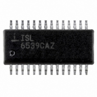
ISL6539CAZ Intersil, ISL6539CAZ Datasheet - Page 10

ISL6539CAZ
Manufacturer Part Number
ISL6539CAZ
Description
IC CTRLR DDR DRAM, SDRAM 28QSOP
Manufacturer
Intersil
Datasheet
1.ISL6539CAZ.pdf
(20 pages)
Specifications of ISL6539CAZ
Applications
Controller, DDR DRAM, SDRAM
Voltage - Input
3.3 ~ 18 V
Number Of Outputs
2
Voltage - Output
0.9 ~ 5.5 V
Operating Temperature
0°C ~ 70°C
Mounting Type
Surface Mount
Package / Case
28-QSOP
Peak Reflow Compatible (260 C)
Yes
Rohs Compliant
Yes
Lead Free Status / RoHS Status
Lead free / RoHS Compliant
Available stocks
Company
Part Number
Manufacturer
Quantity
Price
Part Number:
ISL6539CAZ
Manufacturer:
INTERSIL
Quantity:
20 000
Part Number:
ISL6539CAZ-T
Manufacturer:
INTERSIL
Quantity:
20 000
Current Sensing
The current on the lower MOSFET is sensed by measuring
its voltage drop within its on-time. In order to activate the
current sampling circuitry, two conditions need to be met. (1)
the LGATE is high and (2) the phase pin sees a negative
voltage for regular buck operation, which means the current
is freewheeling through lower MOSFET. For the second
channel of the DDR application, the phase pin voltage needs
to be higher than 0.1V to activate the current sensing circuit
for bidirectional current sensing. The current sampling
finishes at about 400ns after the lower MOSFET has turned
on. This current information is held for current mode control
and overcurrent protection. The current sensing pin can
source up to 260µA. The current sense resistor and OCSET
resistor can be adjusted simultaneously for the same
overcurrent protection level; however, the current sensing
gain will be changed only according to the current sense
resistor value, which will affect the current feedback loop
gain. The middle point of the ISEN current can be at 75µA,
but it can be tuned up and down to fit application needs.
If another channel is switching at the moment the current
sample is finishing, it could cause current sensing error and
phase voltage jitter. In the design stage, the duty cycles and
synchronization have to be analyzed for all the input voltage
and load conditions to reduce the chance of current sensing
error. The relationship between the sampled current and
MOSFET current is given by Equation 4:
Which means the current sensing pin will source current to
make the voltage drop on the MOSFET equal to the voltage
generated on the sensing resistor, plus the internal resistor,
along the ISEN pin current flowing path.
I
SEN
(
R
ISL6539
CS
FIGURE 6. THE INTERNAL COMPENSATOR
+
140
)
UGA T E
OCSET
LGA T E
=
VOUT
VSEN
ISEN
r
DS ON
(
R
Q2
Q1
CS
)
I
D
10
V I N
R
OC
L1
C1
Cz
R1
R2
(EQ. 4)
ISL6539
Feedback Loop Compensation
Both channel PWM controllers have internally compensated
error amplifiers. To make internal compensation possible,
several design measures were taken.
• The ramp signal applied to the PWM comparator has been
• The load current proportional signal is derived from the
The resistor connected to the ISEN pin sets the gain in the
current sensing. The following expression estimates the
required value of the current sense resistor, depending on
the maximum continuous load current, and the value of the
MOSFETs r
current.
Because the current sensing circuit is a sample-and-hold
type, the information obtained at the last moment of the
sampling is being used. This current sensing circuit samples
the inductor current very close to its peak value. The current
feedback essentially injects a resistor R
original LC filter as shown in Figure 7, where the
sample-and-hold effect of the current loop has been ignored.
V
DC operation points.
The value of the injected resistor can be estimated by
Equation 6:
R
is defined as Gm, which is a constant 8dB or 18dB for both
channels in dual switcher applications, when V
3V. Refer to Tables 1 and 2 for the ramp amplitude in
different V
V
output voltage.
R
R
c
IN
i
CS
i
made proportional to the input voltage by the VIN pin. This
keeps the product of the modulator gain and the input
voltage constant even when the input voltage varies.
voltage drop across the lower MOSFET during the PWM
off time interval, and is subtracted from the error amplifier
output signal before the PWM comparator input. This
effectively creates an internal current control loop.
is in kΩ, and r
FIGURE 7. THE EQUIVALENT CIRCUIT OF THE POWER
and V
=
is reflected in Gm. V
=
---------------- -
V
Gm*Vc
V
I
----------------------------------------- -
ramp
MAX
IN
o
IN
are small signal components extracted from its
DS(ON)
75μA
--------------------------- - 4.4kΩ
R
•
r
pin connections. The feed-forward effect of the
CS
STAGE WITH CURRENT LOOP INCLUDED
DS ON
r
+
DS ON
-
(
+
DS
(
140
, assuming the ISEN pin sources 75µA
Ri
)
and R
)
–
•
140Ω
c
CS
is defined as the error amplifier
Lo
are in Ω. V
DCR
i
ESR
IN
in series with the
Co
divided by V
IN
Ro
is above
April 29, 2010
+
-
Vo
FN9144.6
(EQ. 5)
(EQ. 6)
ramp
,


