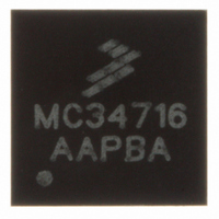
MC34716EP Freescale Semiconductor, MC34716EP Datasheet - Page 14

MC34716EP
Manufacturer Part Number
MC34716EP
Description
IC CONVERTER DDR 26QFN
Manufacturer
Freescale Semiconductor
Datasheet
1.MC34716EP.pdf
(27 pages)
Specifications of MC34716EP
Applications
Converter, DDR
Voltage - Input
3 ~ 6 V
Number Of Outputs
2
Voltage - Output
0.7 ~ 3.6 V
Operating Temperature
-40°C ~ 85°C
Mounting Type
Surface Mount
Package / Case
26-QFN
Output Voltage
0.7 V to 3.6 V
Output Current
5 A
Input Voltage
3 V to 6 V
Switching Frequency
1 MHz
Operating Temperature Range
- 40 C to + 85 C
Mounting Style
SMD/SMT
Lead Free Status / RoHS Status
Lead free / RoHS Compliant
Available stocks
Company
Part Number
Manufacturer
Quantity
Price
Part Number:
MC34716EP
Manufacturer:
FREESCALE
Quantity:
20 000
INTERNAL BIAS CIRCUITS
supply voltages and bias currents for the internal circuitry. It
consists of:
SYSTEM CONTROL AND LOGIC
processes data and reacts to it. Based on the status of the
STBY and SD pins, the system control reacts accordingly and
orders the device into the right status. It also takes inputs
from all of the monitoring/protection circuits and initiates
power up or power down commands. It communicates with
the buck converter to manage the switching operation and
protects it against any faults.
OSCILLATOR
IC digital blocks. It also generates the buck converters
switching frequency. The switching frequency can be
programmed by connecting a resistor divider to the FREQ
pin, between VDDI and GND pins (See
14
34716
FUNCTIONAL DESCRIPTION
FUNCTIONAL INTERNAL BLOCK DESCRIPTION
This block contains all circuits that provide the necessary
• Internal voltage supply regulator: This regulator
• Internal bandgap reference voltage: This supplies the
• Bias circuit: This block generates the bias currents
This block is the brain of the IC where the device
This block generates the clock cycles necessary to run the
supplies the V
analog internal circuits. It is equipped with a Power-On-
Reset (POR) circuit that watches for the right regulation
levels. External filtering is needed on the VDDI pin. This
block will turn off during the shutdown mode.
reference voltage to some of the internal circuitry.
necessary to run all of the blocks in the IC.
DDI
voltage that is used to drive the digital/
MC34716 - Functional Block Diagram
Internal Bias Circuits
Protection Functions
FUNCTIONAL INTERNAL BLOCK DESCRIPTION
Figure
1, page 1).
Figure 7. Block Illustration
System Control and Logic
Supervisory Functions
2 x Buck Converter
Control and
PROTECTION FUNCTIONS
CONTROL AND SUPERVISORY FUNCTIONS
contains the following circuits:
This block contains the following circuits:
• Over-current Limit and Short-circuit Detection: This
• Thermal limit detection: This block monitors the
• Output over-voltage and under-voltage monitoring: This
This block is used to interface with an outside host. It
• Standby Control Input: An outside host can put the
• Shutdown Control Input: An outside host can put the
• Power Good Output Signal: The 34716 can
block monitors the output of the buck converters for
over-current conditions and short-circuit events and
alerts the system control for further command.
temperature of the device for overheating events. If the
temperature rises above the thermal shutdown
threshold, this block will alert the system control for
further commands.
block monitors the buck converters output voltages to
ensure they are within regulation boundaries. If not, this
block alerts the system control for further commands.
34716 device into standby mode (S3 or Suspend-To-
RAM mode) by sending a logic “0” to the STBY pin.
34716 device into shutdown mode (S5 or Suspend-To-
Disk mode) by sending a logic “0” to the SD pin.
communicate to an outside host that a fault has
occurred by pulling the voltage on the PG pin high
through a pull-up resistor.
Tracking and Sequencing
Oscillator
Analog Integrated Circuit Device Data
Freescale Semiconductor


