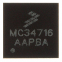
MC34716EP Freescale Semiconductor, MC34716EP Datasheet - Page 13

MC34716EP
Manufacturer Part Number
MC34716EP
Description
IC CONVERTER DDR 26QFN
Manufacturer
Freescale Semiconductor
Datasheet
1.MC34716EP.pdf
(27 pages)
Specifications of MC34716EP
Applications
Converter, DDR
Voltage - Input
3 ~ 6 V
Number Of Outputs
2
Voltage - Output
0.7 ~ 3.6 V
Operating Temperature
-40°C ~ 85°C
Mounting Type
Surface Mount
Package / Case
26-QFN
Output Voltage
0.7 V to 3.6 V
Output Current
5 A
Input Voltage
3 V to 6 V
Switching Frequency
1 MHz
Operating Temperature Range
- 40 C to + 85 C
Mounting Style
SMD/SMT
Lead Free Status / RoHS Status
Lead free / RoHS Compliant
Available stocks
Company
Part Number
Manufacturer
Quantity
Price
Part Number:
MC34716EP
Manufacturer:
FREESCALE
Quantity:
20 000
ERROR AMPLIFIER INVERTING INPUT (INV1, INV2)
V
divider and connect the V
INV2 pin.
OUTPUT VOLTAGE DISCHARGE PATH (VOUT1,
VOUT2)
pins. It only serves as the output discharge path once the SD
signal is asserted.
INTERNAL SUPPLY VOLTAGE OUTPUT (VDDI)
Connect a 1.0 µF, 6.0 V low ESR ceramic filter capacitor
between this pin and the GND pin. Filtering any spikes on this
output is essential to the internal circuitry stable operation.
SIGNAL GROUND (GND)
referenced to this pin voltage.
INPUT SUPPLY VOLTAGE (VIN)
the device to operate properly.
POWER GOOD OUTPUT SIGNAL (PG)
report the status of the device to a host. This output activates
after a successful power up sequence and stays active as
long as the device is in normal operation and is not
experiencing any faults. This output activates after a 10ms
delay and must be pulled up by an external resistor to a
supply voltage like V
Analog Integrated Circuit Device Data
Freescale Semiconductor
DDQ
Buck converter error amplifier inverting input. Connect the
Buck converters output voltage are connected to these
This is the output of the internal bias voltage regulator.
Analog ground of the IC. Internal analog signals are
IC power supply input voltage. Input filtering is required for
This is an active low open drain output that is used to
voltage (channel 1) to INV1 pin through a resistor
IN
.
TT
voltage (channel 2) directly to
STANDBY INPUT (STBY)
Standby mode. If left unconnected or tied to the VIN pin, the
device will be in Normal mode. The pin has an internal pull-
up of 1.5 MΩ. This input accepts the S3 (Suspend-To-RAM)
control signal.
SHUTDOWN INPUT (SD)
Shutdown Mode. If left unconnected or tied to the VIN pin, the
device will be in Normal mode. The pin has an internal pull-
up of 1.5 MΩ. This input accepts the S5 (Suspend-To-Disk)
control signal.
REFERENCE VOLTAGE OUTPUT (VREFOUT)
1/2 V
output is used as the V
against any noise. Connect a 0.1 µF, 6.0 V low ESR ceramic
filter capacitor between this pin and the GND pin and
between this pin and V
reference voltage for the buck converter error amplifier.
REFERENCE VOLTAGE INPUT (VREFIN)
at this pin.
FREQUENCY ADJUSTMENT INPUT (FREQ)
by connecting this pin to an external resistor divider between
VDDI and GND pins. The default switching frequency (FREQ
pin connected to ground, GND) is set at 1.0 MHz.
CHANNEL 1 SOFT START ADJUSTMENT INPUT
(ILIM1)
voltage between 1.25 V and V
If this pin is tied to the GND pin, the device will be in
If this pin is tied to the GND pin, the device will be in
This is a buffered reference voltage output that is equal to
The output of channel two will track 1/2 the voltage applied
The buck converters switching frequency can be adjusted
Channel one Soft Start can be adjusted by applying a
REFIN
. It has a 10 mA current drive capability. This
REF
DDQ
voltage rail and should be filtered
rail. V
FUNCTIONAL PIN DESCRIPTION
DDI
FUNCTIONAL DESCRIPTION
REFOUT
.
is also used as the
34716
13


