ISL6306IRZ Intersil, ISL6306IRZ Datasheet
ISL6306IRZ
Specifications of ISL6306IRZ
Available stocks


Related parts for ISL6306IRZ

ISL6306IRZ Summary of contents
Page 1
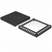
... ISL6306CRZ* ISL6306 CRZ 6x6 QFN L40.6x6 ISL6306CRZ-TK ISL6306 CRZ 6x6 QFN L40.6x6 ISL6306IRZ* ISL6306 IRZ - 6x6 QFN L40.6x6 *Add “-T” suffix for tape and reel. Please refer to TB347 for details on reel specifications. NOTE: These Intersil Pb-free plastic packaged products employ special Pb-free material sets ...
Page 2
Pinout VID6 VID5 VID4 VID3 VID2 VID1 VID0 VRSEL OFS DAC 2 ISL6306 ISL6306 (40 LD QFN) TOP VIEW GND ...
Page 3
ISL6306CR Block Diagram VDIFF VR_RDY RGND x1 VSEN OVP SOFT-START +175mV FAULT LOGIC SS OFFSET OFS REF DAC VRSEL VID7 VID6 VID5 DYNAMIC VID4 VID D/A VID3 VID2 VID1 VID0 COMP FB IDROOP VR_HOT THERMAL MONITORING VR_FAN TM 3 ISL6306 ...
Page 4
Typical Application - 4-Phase Buck Converter with r FB COMP REF IDROOP DAC V DIFF VSEN VCC RGND VTT EN_VTT VR_RDY ISL6306 ISEN1+ VID7 ISEN1- VID6 PWM1 PWM2 VID5 ISEN2+ VID4 ISEN2- VID3 PWM3 ISEN3+ VID2 ISEN3- VID1 PWM4 VID0 ...
Page 5
Typical Application - 4-Phase Buck Converter with r FB COMP REF IDROOP DAC VDIFF VSEN VCC RGND VTT EN_VTT VR_RDY ISL6306 ISEN1+ VID7 ISEN1- VID6 PWM1 PWM2 VID5 ISEN2+ VID4 ISEN2- VID3 PWM3 ISEN3+ VID2 ISEN3- VID1 PWM4 VID0 ISEN4+ ...
Page 6
Typical Application - 4-Phase Buck Converter with DCR Sensing and External TCOMP FB COMP REF IDROOP DAC V DIFF VSEN VCC RGND VTT EN_VTT VR_RDY ISL6306 ISEN1+ VID7 ISEN1- VID6 PWM1 PWM2 VID5 ISEN2+ VID4 ISEN2- VID3 PWM3 ISEN3+ VID2 ...
Page 7
Typical Application - 4-Phase Buck Converter with DCR Sensing and Integrated TCOMP FB COMP REF IDROOP DAC V DIFF VSEN VCC RGND VTT EN_VTT VR_RDY ISL6306 ISEN1+ VID7 ISEN1- VID6 PWM1 PWM2 VID5 ISEN2+ VID4 ISEN2- VID3 PWM3 ISEN3+ VID2 ...
Page 8
... Supply Voltage (VCC +5V ±5% Ambient Temperature ISL6306CRZ 0°C to +70°C ISL6306IRZ . . . . . . . . . . . . . . . . . . . . . . . . . . . . . .-40°C to +85°C CAUTION: Do not operate at or near the maximum ratings listed for extended periods of time. Exposure to such conditions may adversely impact product reliability and result in failures not covered by warranty. ...
Page 9
... DAC Source Current DAC Sink Current REF Source Current REF Sink Current PIN-ADJUSTABLE OFFSET Voltage at OFS Pin of ISL6306CRZ Voltage at OFS Pin of ISL6306IRZ OSCILLATORS Accuracy of Switching Frequency Setting Adjustment Range of Switching Frequency (Note 4) Soft-Start Ramp Rate Adjustment Range of Soft-start Ramp Rate (Note 4) ...
Page 10
Electrical Specifications Operating Conditions: VCC = 5V, Unless Otherwise Specified (Continued) PARAMETER Leakage Current of VR_FAN VR_FAN Low Voltage Leakage Current of VR_HOT VR_HOT Low Voltage VR READY AND PROTECTION MONITORS Leakage Current of VR_RDY VR_RDY Low Voltage Undervoltage Threshold ...
Page 11
... Dynamic VID™ operations. PWM1, PWM2, PWM3, PWM4 Pulse width modulation outputs. Connect these pins to the PWM input pins of the Intersil driver IC. The number of active channels is determined by the state of PWM3 and PWM4. Tie PWM3 to VCC to configure for 2-phase operation. Tie PWM4 to VCC to configure for 3-phase operation. ISEN1+, ISEN1- ...
Page 12
When configured for r current sensing, the ISEN1-, DS(ON) ISEN2-, ISEN3-, and ISEN4- pins are grounded at the lower MOSFET sources. The ISEN1+, ISEN2+, ISEN3+, and ISEN4+ pins are then held at a virtual ground. Therefore, a resistor, connected between ...
Page 13
IL1 + IL2 + IL3, 7A/DIV IL1, 7A/DIV PWM1, 5V/DIV PWM2, 5V/DIV IL3, 7A/DIV PWM3, 5V/DIV 1µs/DIV FIGURE 1. PWM AND INDUCTOR-CURRENT WAVEFORMS FOR 3-PHASE CONVERTER To understand the reduction of ripple current amplitude in the multiphase circuit, examine Equation ...
Page 14
V , minus the current correction signal relative to the COMP sawtooth ramp as illustrated in Figure 7. When the modified V voltage crosses the sawtooth ramp, the PWM ...
Page 15
... Channel current balance is achieved by comparing the sampled current of each channel to the average current to make an appropriate adjustment to DS(ON) the WPM duty cycle of each channel. Intersil’s patented current-balance method is illustrated in Figure 7. In the figure, the average current combines with the Channel 1 current (I ) ...
Page 16
... The output of the error amplifier (V COMP sawtooth waveform to generate the PWM signals. The PWM signals control the timing of the Intersil MOSFET drivers and regulate the converter output to the specified reference voltage. The internal and external circuitry, which control voltage regulation, are illustrated in Figure 8. ...
Page 17
TABLE 1. VR10 VID TABLE (WITH 6.25mV EXTENSION) VID4 VID3 VID2 VID1 VID0 VID5 400mV 200mV 100mV 50mV 25mV 12.5mV ...
Page 18
TABLE 1. VR10 VID TABLE (WITH 6.25mV EXTENSION) (Continued) VID4 VID3 VID2 VID1 VID0 VID5 400mV 200mV 100mV 50mV 25mV 12.5mV ...
Page 19
TABLE 2. VR11 VID 8 BIT (Continued) VID7 VID6 VID5 VID4 VID3 VID2 VID1 VID0 VOLTAGE ...
Page 20
TABLE 2. VR11 VID 8 BIT (Continued) VID7 VID6 VID5 VID4 VID3 VID2 VID1 VID0 VOLTAGE ...
Page 21
Load-Line Regulation Some microprocessor manufacturers require a precisely- controlled output resistance. This dependence of output voltage on load current is often termed “droop” or “load line” regulation. By adding a well controlled output impedance, the output voltage can effectively be ...
Page 22
... REF ISL6306 becomes enabled. The schematic in Figure 10 demonstrates sequencing the ISL6306 with the ISL66xx (EQ. 13) family of Intersil MOSFET drivers, which require 12V bias. 3. The voltage on EN_VTT must be higher than 0.875V to enable the controller. This pin is typically connected to the output of VTT VR. ...
Page 23
... At the inception of an overvoltage event, all PWM outputs are commanded low instantly (less than 20ns) until the voltage at VDIFF falls below 0.4V. This causes the Intersil drivers to turn on the lower MOSFETs and pull the output voltage below a level that might cause damage to the load. ...
Page 24
... SW At the beginning of overcurrent shutdown, the controller places all PWM signals in a high-impedance state within 20ns commanding the Intersil MOSFET driver ICs to turn off both upper and lower MOSFETs. The system remains in this state a period of 4096 switching cycles. If the controller is still enabled at the end of this wait period, it will attempt a soft- start ...
Page 25
TEMPERATURE TM CC 100 TEMPERATURE (°C) FIGURE 15. THE RATIO OF TM VOLTAGE TO NTC TEMPERATURE WITH RECOMMENDED PARTS TM 0.39*V CC 0.33*V CC ...
Page 26
Depending on the location of the NTC and the airflow, the NTC may be cooler or hotter than the current sense component. TCOMP pin voltage can be utilized to correct the temperature difference between NTC and the current sense component. ...
Page 27
... It is assumed that the reader is familiar with many of the basic skills and techniques referenced below. In addition to this guide, Intersil provides complete reference designs that include schematics, bills of materials, and example board layouts for all common microprocessor applications ...
Page 28
Equations 25, 26, and 27. Since the power equations depend on MOSFET parameters, choosing the correct MOSFETs can be an iterative process involving repetitive solutions to the loss equations for different MOSFETs and different switching frequencies ⎛ ...
Page 29
Case 1: 0 2π LC 2π P -------------------------------------- - C FB 0.75V IN 0.75V ------------------------------------- - C 2π P ≤ ------------------- f ...
Page 30
Output Filter Design The output inductors and the output capacitor bank together to form a low-pass filter responsible for smoothing the pulsating voltage at the phase nodes. The output filter also must provide the transient energy until the regulator can ...
Page 31
... Align the output inductors and MOSFETs such that space between the components is minimized while creating the PHASE 0.8 1.0 plane. Place the Intersil MOSFET driver IC as close possible to the MOSFETs they control to reduce the parasitic ...
Page 32
... Accordingly, the reader is cautioned to verify that data sheets are current before placing orders. Information furnished by Intersil is believed to be accurate and reliable. However, no responsibility is assumed by Intersil or its subsidiaries for its use; nor for any infringements of patents or other rights of third parties which may result from its use ...
Page 33
Package Outline Drawing L40.6x6 40 LEAD QUAD FLAT NO-LEAD PLASTIC PACKAGE Rev 3, 10/06 6.00 6 PIN 1 INDEX AREA (4X) 0.15 TOP VIEW ( TYP ) ( TYPICAL RECOMMENDED LAND PATTERN 33 ...