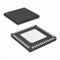
ISL9502CRZ Intersil, ISL9502CRZ Datasheet - Page 19

ISL9502CRZ
Manufacturer Part Number
ISL9502CRZ
Description
IC CTRLR PWM 2PHASE GPU 48-QFN
Manufacturer
Intersil
Datasheet
1.ISL9502CRZ-T.pdf
(24 pages)
Specifications of ISL9502CRZ
Pwm Type
Controller
Number Of Outputs
1
Frequency - Max
500kHz
Voltage - Supply
4.75 V ~ 5.25 V
Buck
Yes
Boost
No
Flyback
No
Inverting
No
Doubler
No
Divider
No
Cuk
No
Isolated
No
Operating Temperature
-10°C ~ 100°C
Package / Case
48-VQFN
Frequency-max
500kHz
Lead Free Status / RoHS Status
Lead free / RoHS Compliant
Duty Cycle
-
Once the NTC thermistor resistor is determined, the series
resistor can be derived by:
Once R
at T
One example of using Equations 9, 10 and 11 to design a
thermal throttling circuit with the temperature hysteresis
100°C to 105°C is illustrated as follows. Since T
and T
the Equation 9 gives the required NTC nominal resistance as
In fact, the datasheet gives the resistor ratio value at 100°C
to 105°C, which is 0.03956 and 0.03322 respectively. The b
value 4700K in Panasonic datasheet only covers to 85°C.
Therefore, using Equation 10 is more accurate for 100°C
design, the required NTC nominal resistance at 25°C is
402kΩ. The closest NTC resistor value from manufacturer is
470kΩ. So the series resistance is given by Equation 11 as
follows:
Furthermore, the NTC resistance at T
From the NTC datasheet, it can be concluded that the actual
temperature T
calculated to be 97.7°C. Check the NTC datasheet to decide
whether Equation 9 or Equation 10 can accurately represent
the NTC resistor value at the designed temperature range.
Therefore, the NTC branch is designed to have a 470k NTC
and 4.02k resistor in series. The part number of the NTC
thermistor is ERTJ0EV474J. It is a 0402 package. The NTC
thermistor should be placed in the spot which gives the best
indication of the temperature of voltage regulator circuit. The
actual hysteresis temperature is about 105°C and 97°C.
Static Mode of Operation - Static Droop Using DCR
Sensing
As previously mentioned, the ISL9502 has an internal
differential amplifier which provides for very accurate voltage
regulation at the die of the processor. The load line
regulation is also accurate for both two-phase and single-
phase operation. The process of selecting the components
for the appropriate load line droop is explained here.
R
R
T
R
R
R
2_actual
S
NTC_T
NTC_To
S
NTC_T2
=
2
=
and the actual T
2
19.67kΩ R
1.18V
--------------- - R
60µA
NTCTo
= 100°C, if we use a Panasonic NTC with B = 4700,
2
=
=
=
=
---------------------------------------------------------------------------------- - 273
1
-- -
b
2.55kΩ
396kΩ
2.55kΩ
–
ln
2
and R
–
⎛
⎜
⎝
NTC
R
-------------------------
is about 97°C. If using the Equation 13, T
R
NTC_T
NTC_105°C
NTCTo
(
+
+
T1
s
R
R
is designed, the actual NTC resistance
2
NTC_T
NTC_T1
)
2
temperature can be found in:
=
⎞
⎟
⎠
1
19.67kΩ R
+
1
=
1
19
⁄
(
19.67kΩ 15.65kΩ
=
273
18.16kΩ
–
+
2
To
NTC_T
is given by Equation 12.
–
)
–
1
1
=
= 105°C
4.067kΩ
(EQ. 12)
(EQ. 13)
(EQ. 11)
2
is
ISL9502
For DCR sensing, the process of compensation for DCR
resistance variation to achieve the desired load line droop
has several steps and is somewhat iterative.
The two-phase solution using DCR sensing is shown in
Figure 23. There are two resistors connecting to the
terminals of inductor of each phase. These are labelled RS
and RO. These resistors are used to obtain the DC voltage
drop across each inductor. Each inductor will have a certain
level of DC current flowing through it, and this current when
multiplied by the DCR of the inductor creates a small DC
voltage drop across the inductor terminal. When this voltage
is summed with the other channels DC voltages, the total DC
load current can be derived.
RO is typically 1 to 10Ω. This resistor is used to tie the
outputs of all channels together and thus create a summed
average of the local CORE voltage output. RS is determined
through an understanding of both the DC and transient load
currents. This value will be covered in the next section.
However, it is important to keep in mind that the output of
each of these RS resistors are tied together to create the
VSUM voltage node. With both the outputs of RO and RS
tied together, the simplified model for the droop circuit can
be derived. This is presented in Figure 26.
Figure 26 shows the simplified model of the droop circuitry.
Essentially one resistor can replace the RO resistors of each
phase and one RS resistor can replace the RS resistors of
each phase. The total DCR drop due to load current can be
replaced by a DC source, the value of which is given by:
For the convenience of analysis, the NTC network
comprised of Rntc, Rseries and Rpar, given in Figure 23, is
labelled as a single resistor Rn in Figure 26.
The first step in droop load line compensation is to adjust
Rn, RO
exists even at light loads between the VSUM and VO' nodes.
As a rule of thumb we start with the voltage drop across the
Rn network, VN, to be 0.5-0.8 times V
provides for a fairly reasonable amount of light load signal
from which to arrive at droop.
The resultant NTC network resistor value is dependent on
the temperature and given by
For simplicity, the gain of Vn to the V
G1, also dependent on the temperature of the NTC
thermistor.
V
R
DCR_EQU
n
T ( )
=
EQV
(
--------------------------------------------------------------
R
R
series
series
=
and RS
I
-------------------------------- -
OUT
+
+
R
R
•
2
EQV
ntc
ntc
DCR
) R
+
•
such that sufficient droop voltage
R
par
par
dcr_equ
DCR_EQU
is defined by
. This ratio
July 17, 2006
(EQ. 14)
(EQ. 15)
FN9275.1


